High Density Interconnect (HDI) PCB circuit board is a circuit board with relatively high line distribution density using microblind and buried via technology. The most effective way to increase board density is to reduce the number of vias and precisely place blind and buried vias to meet this requirement, resulting in an HDI board.
This is a process that includes wires on the inner layer and wires on the outer layer, and then uses holes and metallization in the holes to achieve the function of bonding between the inner layers of each layer. HDI PCB is a printed circuit board with a higher wiring density per unit surface areathan a standard PCB board. HDI PCB uses some or all of the following features to reduce the size of the PCB:
If you have any requirements for PCB/ PCBA/Components, please contact us and we will reply to you as soon as possible!
We Provide High-end Quality Rigid PCB, Flexible PCB, Rigid-flex PCB, Metal Core PCB; 2-64L Mutilayer PCB; HDI PCB (2+N+2); High Frequency PCB Manufacturing and Assembly.
 中文
中文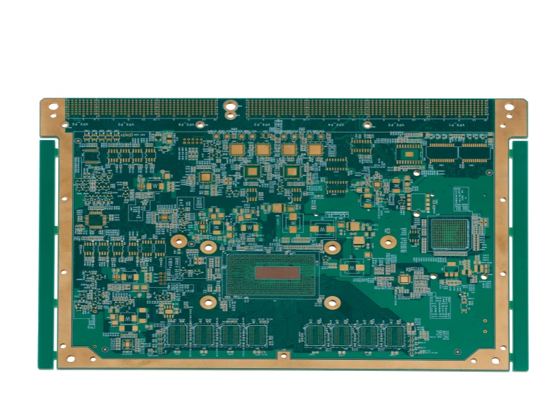


 English


