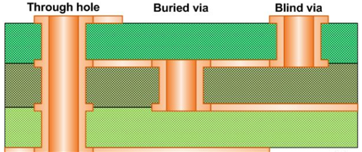
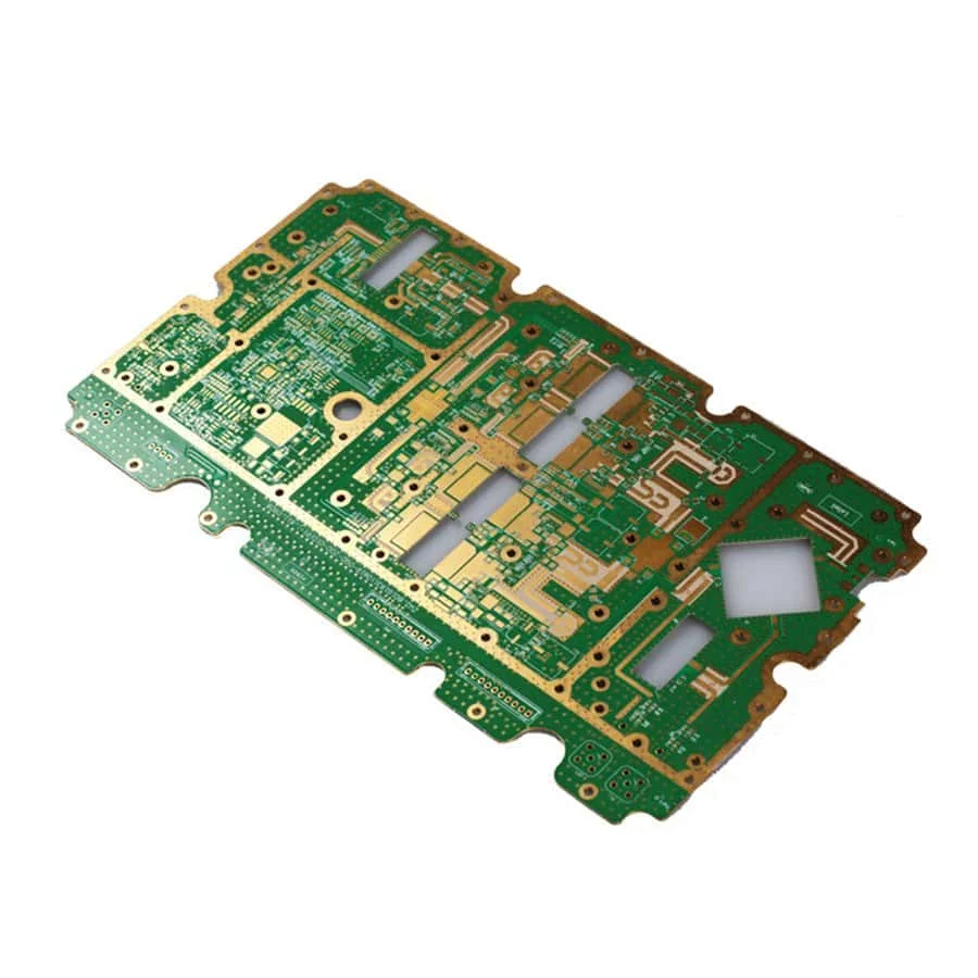
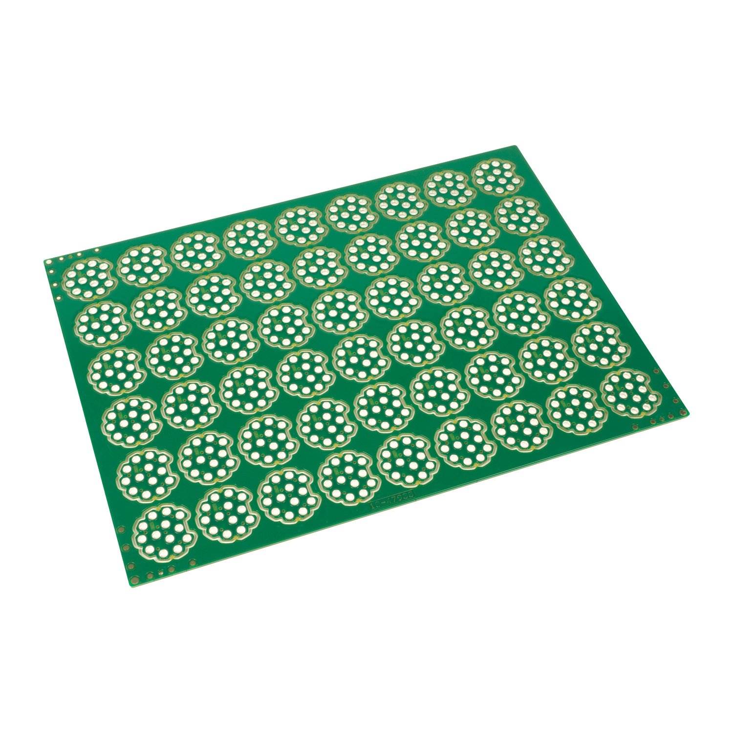
Blind vias are vias that connect the surface layer and the inner layer without penetrating the entire board. Blind vias are located on the top and bottom surfaces of a printed circuit board and have a certain depth. They are used to connect the surface circuit and the inner circuit below. The depth of the hole usually does not exceed a certain ratio (aperture).
The difference between through hole, blind vias hole and buried hole
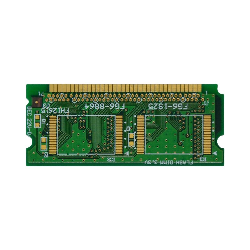
Through hole: Plating Through Hole, also known as PTH, is the most common type. If you hold the PCB up to the light, the hole where you can see the light is a “through hole”. This is also the simplest type of hole, because when making it, you only need to use a drill or laser to drill all the holes in the circuit board, and the cost is relatively cheap. However, in contrast, some circuit layers do not need to connect these through holes. For example, we have a six-story house. I bought the third and fourth floors. I want to design a staircase inside to connect only the third and fourth floors. For me, the space on the fourth floor is virtually occupied by the original staircase connecting the first floor to the sixth floor. So although through holes are cheap, sometimes they will use up more space on the PCB.
Blind Via Hole:The outermost circuit of the PCB is connected to the adjacent inner layer with a plated hole. Because you can’t see the opposite side, it is called “blind via”. In order to increase the space utilization of the PCB circuit layer, the “blind hole” process came into being. This production method requires special attention to the depth of the drilling (Z2 axis) to be just right. This method often makes it difficult to electroplate in the hole, so almost no manufacturer adopts it; you can also drill holes in the circuit layers that need to be connected in advance when they are in individual circuit layers, and then glue them together, but it requires more precise positioning and alignment devices.
Buried hole:Buried hole, the connection of any circuit layer inside the PCB but not connected to the outer layer. This process cannot be achieved by drilling after bonding. It must be drilled in individual circuit layers. After partially bonding the inner layer, it must be electroplated first, and finally all can be bonded. It takes more time than the original “through hole” and “straight hole”, so the price is also the most expensive. This process is usually only used in high-density (HDD circuit boards to increase the available space of other circuit layers.
If you have any requirements for PCB/ PCBA/Components, please contact us and we will reply to you as soon as possible!
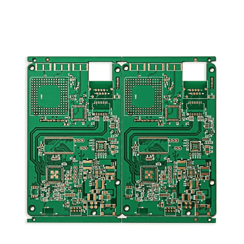
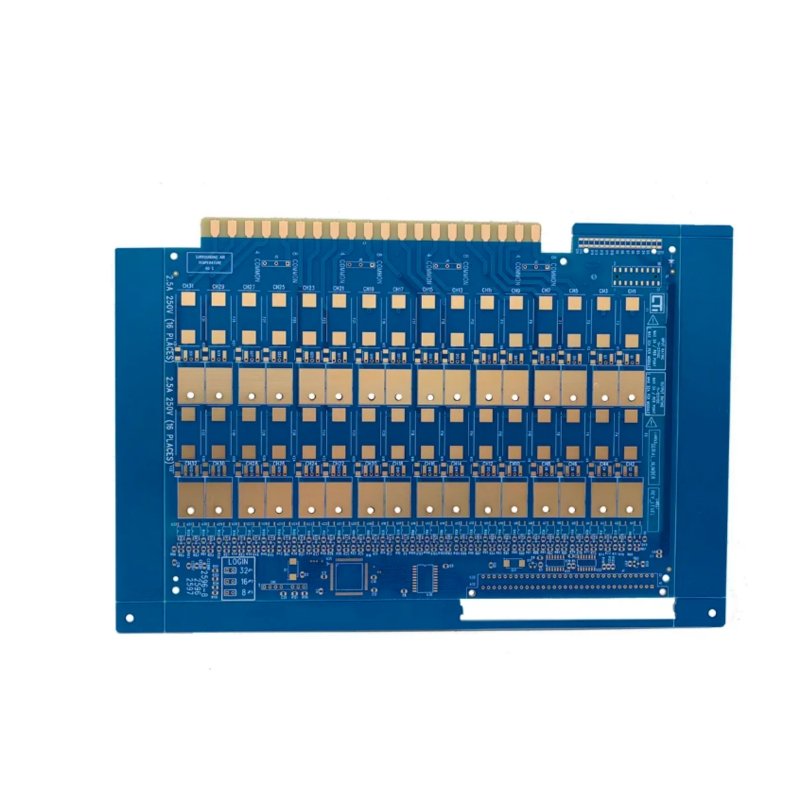
We Provide High-end Quality Rigid PCB, Flexible PCB, Rigid-flex PCB, Metal Core PCB; 2-64L Mutilayer PCB; HDI PCB (2+N+2); High Frequency PCB Manufacturing and Assembly.
 中文
中文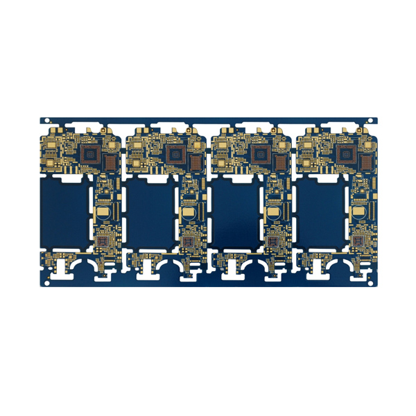


 English


