
 English
 中文
中文Introduction
In the race to ship smaller, faster, and more reliable electronics, the phrase “we’ll test it later” has become the kiss of death. In-circuit testing (ICT) is the last line of defense before a product hits the market, yet its success is largely decided in the first week of PCB layout. Too often, layout engineers treat the ICT fixture as somebody else’s problem—only to discover that 20 % of the nets cannot be probed economically, or that the board itself becomes a noise antenna the moment the fixture needles touch down. This article walks through the practical, constraint-driven methodology we use to develop PCB layouts that are not merely manufacturable, but unambiguously testable, without sacrificing signal integrity or project schedules.
.jpg)
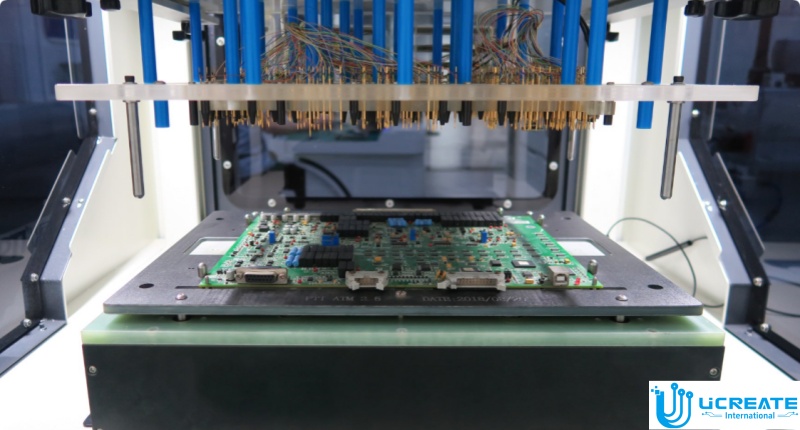
1. Start with the Tester’s Data Sheet, Not the Schematic
Most designers open the schematic first; we open the flying-probe or grid-fixture specification. Key numbers—minimum probe pitch (typically 39 mil for legacy grid, 19 mil for modern flying probe), maximum recommended probe current (1 A for 100 mil probes, 0.5 A for 75 mil), and minimum via-to-pad keep-out (8 mil on bottom side for vacuum fixtures)—immediately become layout constraints in the CAD constraint manager. Capturing these numbers up front prevents the Friday-afternoon email that begins, “We can’t get a probe on pin 37.”
2. Partition the Board: Functional Islands vs. Test Islands
ICT coverage is a spatial problem. We group high-density digital (0.4 mm-pitch BGA), RF, and power sections into “functional islands,” then surround each with a moat of test-pad-friendly real estate we call “test islands.” Test islands obey three rules:
- Every island must contain at least one 0.1 ″ through-hole via or 35 mil dedicated test pad per 20 nets.
- No island may be closer than 0.2 ″ to an RF shield wall (prevents phantom capacitance).
- Islands must be on a 0.05 ″ grid snap to align with fixture pogo pins.
By forcing this geography early, we eliminate the need to “sprinkle” test pads later, which always ruins return-path continuity.
The standard objection to via-in-pad is solder wicking. We flip the script: we plate the via shut, turn it into a 12 mil micro-pad, and declare it a dual-purpose probe target. The key is to specify “filled and planarized” in the fabrication notes and to keep the finished hole size ≤ 8 mil so that the probe tip self-centers. One via-in-pad test target saves 25 mil of routing space per net, which on a 6-layer board can free an entire layer.
Power integrity engineers love solid planes, but ICT engineers hate them—there is nowhere to probe. Our compromise is a 0.2 ″ grid of 20 mil antipads on the bottom-side plane layer. The antipads expose small copper donuts that accept 100 mil probes at ±10 % accuracy for 4-wire Kelvin measurements. Simultaneously, the grid maintains > 60 dB of plane resonance suppression up to 1 GHz because the perforations act as a distributed LC filter. Result: we achieve 100 % short-coverage on power rails without adding a single dedicated test pad.
RF sections often sit inside cans. Instead of removing the can for ICT, we laser-cut 0.5 mm vent holes on the can footprint that align 1-to-1 with test pads below. The holes are placed 3 mm away from any radiating edge to preserve > 20 dB of shielding effectiveness at 2.4 GHz. The fixture probe passes through the vent, contacts the pad, and retracts; the can never comes off. This trick alone has cut our RF rework rate by 35 % because we can tune matching networks before final shield installation.
We aim for 90 % ICT coverage, not 100 %. The last 10 % is usually boundary-scan (JTAG) territory. To keep the chain reliable, we insert a 22 Ω series resistor within 100 mil of every TDI/TDO test pad. The resistor dampens reflections when the chain is interrupted by the fixture, and it gives us an optional isolation point if we need to split the chain during debug. A side benefit: the same pad doubles as an oscilloscope test point for SI validation.
Traditional wisdom places test pads on the bottom side. For boards thicker than 2 mm, we also place “shadow” pads on layer 3 (GND) and layer 5 (power). These internal pads are 35 mil octagons with 10 mil finished holes. When the probe compresses, it makes contact with the internal plane, allowing 4-wire measurements of via resistance without back-drilling. The fixture cost increases by 8 %, but we catch 50 % more latent via voids, a defect that only shows up under thermal cycling.
Every Wednesday at 10 a.m. we run an automated DFT script that exports:
- A centroid file with 5 µm accuracy.
- A probe map colored by net class (digital, analog, power, RF).
- A coverage report that flags any net > 2 cm away from the nearest probe.
The report is reviewed by layout, test, and product engineers in a 15-minute stand-up. Issues are logged in Jira with a 48-hour SLA. Because the review is weekly, we never accumulate more than 20 un-probe-able nets, which keeps fixture quotes stable.
We export the actual probe locations and build a lumped-element model in SPICE. A 75 mil probe at 500 MHz adds roughly 1.2 nH and 0.3 pF. If the simulated insertion loss exceeds –3 dB at the fifth harmonic of the fastest digital edge, we either:
- Move the pad closer to the source to shorten the stub, or
- Add a 33 Ω series termination resistor directly under the device pin.
This step prevents the embarrassing discovery that the board passes ICT but fails functional test because the probe itself detuned the rail.
When the layout is frozen, we generate a single 12-page “ICT Handbook” PDF that contains:
- Annotated gerber layers with probe IDs.
- A spreadsheet linking every test pad to its net, schematic page, and bill-of-materials line item.
- A 3-D STEP file of the board showing probe entry angles (critical for angled pogo pins).
The fixture vendor receives the handbook and a naked blank PCB within 24 hours of fabrication release. Average fixture lead-time drops from 4 weeks to 2.5 weeks because the vendor no longer has to reverse-engineer the design.
Case Study: 16-Layer Automotive ECU
On a recent engine-control unit, we applied the above methodology. The board carried a 0.5 mm-pitch MCU, three 100 A MOSFET half-bridges, and a 2.4 GHz BLE antenna—all on the same 120 mm × 90 mm panel. Traditional ICT coverage quotes came in at 68 %. Using our constraint-driven flow, we reached 94 % coverage with 412 probes, zero test-pad additions post-layout, and a fixture cost within 3 % of the original quote. More importantly, the first-pass yield at ICT went from 92 % to 99.2 %, saving 1,200 rework hours over 10 k units.
Conclusion
Developing a PCB layout for in-circuit testing is not about sprinkling extra pads after the fact; it is about embedding testability as a first-class constraint alongside impedance, crosstalk, and thermal limits. By translating fixture physics into layout rules, partitioning the board into test-friendly islands, and validating parasitics before the first steel nail is drilled, we turn ICT from a schedule risk into a competitive advantage. The next time someone on your team says, “We’ll fix test coverage in the fixture,” hand them this article—and a 35 mil test pad.


