
 English
 中文
中文In the fast-paced world of electronics manufacturing, a critical truth often goes unnoticed: up to 70% of a product’s total manufacturing cost is determined during the design phase. Every decision made at the schematic level ripples through production, assembly, testing, and ultimately, your bottom line. This is where PCB DFA (Design for Assembly) emerges as not just a methodology, but a competitive weapon.
PCB DFA represents a paradigm shift—from designing circuits that merely function, to designing products that can be manufactured efficiently, reliably, and cost-effectively at scale. In an era where time-to-market pressures intensify and supply chains grow more complex, mastering DFA principles separates industry leaders from followers.
Understanding PCB DFA: Beyond the Basics

The Strategic Imperative: Why PCB DFA Matters Now
The electronics industry is undergoing unprecedented transformation. Miniaturization continues unabated, with components shrinking while functionality expands. High-Density Interconnect (HDI) boards, flexible circuit boards, and complex multi-layer designs are now standard rather than exceptional. Simultaneously, manufacturers face mounting pressure to reduce costs, improve quality, and accelerate delivery timelines.
1. Dramatic Cost Reduction
Industry research consistently demonstrates that assembly costs account for a significant portion of total PCB manufacturing expenses. By implementing DFA principles, companies can achieve cost reductions of 20-50% in assembly operations. These savings stem from multiple sources: reduced labor requirements through automation compatibility, lower defect rates minimizing rework, decreased component count through strategic consolidation, and optimized material utilization.
2. Accelerated Time-to-Market
3. Enhanced Quality and Reliability
4. Supply Chain Resilience
Core Principles of Effective PCB DFA
1. Component Selection and Standardization
- Standardized packaging: Favoring widely-used component packages (0402, 0603, 0805 for passives; standard QFN, QFP, BGA footprints for ICs) ensures compatibility with automated assembly equipment and reduces tooling requirements.
- Consolidation strategy: Where possible, standardizing on common values and packages reduces inventory complexity and enables bulk purchasing advantages.
- Availability-aware selection: Incorporating real-time supply chain data into component selection prevents costly redesigns due to obsolescence or shortage.
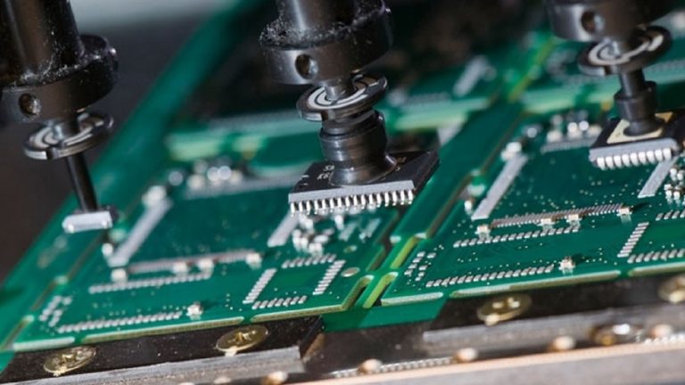
2. Layout Optimization for Automated Assembly
- Consistent component orientation: Aligning polarized components in uniform directions simplifies programming and reduces placement errors.
- Adequate spacing: Maintaining sufficient clearance between components for nozzle access, vision system recognition, and thermal management during reflow.
- Panelization strategy: Designing boards for efficient panel layouts maximizes material utilization and throughput while facilitating depaneling processes.
- Fiducial placement: Strategic placement of fiducial markers enables precise machine alignment, critical for fine-pitch components and high-density designs.
3. Thermal and Mechanical Considerations
- Thermal relief patterns: Proper thermal management in pad designs ensures consistent solder joint formation while maintaining electrical and thermal performance.
- Mechanical stability: Component placement should consider mechanical stresses during assembly, testing, and end-use, particularly for large or heavy components.
- Warpage control: Board thickness, layer stackup, and copper distribution must be optimized to minimize warpage during the assembly thermal cycle.
4. Design for Inspection and Test
- Automated Optical Inspection (AOI): Clear sightlines to critical solder joints and component features enable automated quality verification.
- In-Circuit Test (ICT): Adequate test point access and spacing support comprehensive electrical verification.
- Functional test interfaces: Strategic placement of test connectors and programming interfaces streamlines final validation.
5. Advanced DFA: Embracing Emerging Technologies
- High-Density Interconnect (HDI) Optimization
HDI boards with microvias, blind/buried vias, and fine-line geometries require specialized DFA approaches. Laser-drilled microvias demand precise pad sizing and annular ring control. Sequential lamination processes necessitate careful material selection and layer stackup optimization to maintain registration accuracy through multiple thermal cycles.
- Flexible and Rigid-Flex Design
- RF and High-Speed Digital Integration
- The Economic Case: Quantifying DFA Impact
The return on investment for DFA implementation extends across multiple dimensions:
- Direct Manufacturing Savings: Labor cost reduction through automation compatibility typically yields 15-30% savings in high-volume production. Material optimization through efficient panelization and reduced scrap contributes additional 5-10% cost reduction.
- Quality Cost Avoidance: Industry data indicates that defect costs increase exponentially as products progress through the value chain. A defect caught during design costs $1 to fix; in production, $10; in the field, $100 or more. DFA’s focus on prevention rather than correction delivers substantial quality cost avoidance.
- Inventory and Working Capital Benefits: Component standardization and design consolidation reduce SKU complexity, enabling inventory reduction of 20-40% while improving availability.
- Time-to-Revenue Acceleration: Streamlined production ramps and reduced engineering change orders accelerate market entry, capturing revenue earlier and extending product lifecycles in fast-moving markets.


