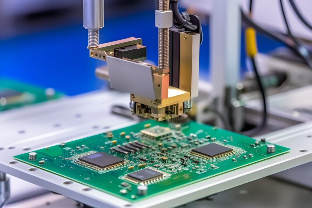
Introduction of Single-Sided PCB
- Structure and Functionality
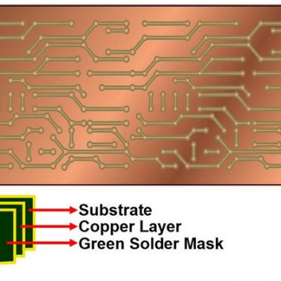
A single-sided PCB board is composed of a single layer of substrate material, typically made of fiberglass-reinforced epoxy resin known as FR-4. On one side of the substrate, a thin layer of copper is laminated, forming the conductive pathways for electrical signals. The copper layer is etched to create the desired circuit pattern, leaving behind the required traces and pads for component mounting.
- Advantages
Single layer PCB offer several advantages that make them a popular choice for various applications. One of the key advantages is their simplicity. With only one layer of conductive material, the design and manufacturing processes are streamlined, resulting in faster production cycles and lower costs. The simplicity of single-sided board also makes them ideal for circuits with fewer components, reducing the complexity of routing and assembly.
Cost-effectiveness is another significant advantage of single-sided circuit baord. As they require fewer materials and manufacturing steps compared to multilayer boards, single-sided PCBs are more economical, particularly for low-cost products or applications with budget constraints.
- Applications
These circuit boards have wide applications in numerous industries. They are commonly used in consumer electronics, such as calculators, remote controls, and basic control PCB. Additionally, They are employed in automotive systems, industrial controls, lighting applications, and more.
Their suitability for simple electronic circuits makes single-sided PCB an excellent choice for prototypes, small-scale production runs, and applications where circuit complexity is relatively low. They are also favored in scenarios where cost considerations play a significant role.
Navigating the Manufacturing Process of Single-Sided PCB
Let’s delve into the step-by-step manufacturing process of producing high-quality single PCB. Each stage is crucial in ensuring the reliability and functionality of the final product. By gaining insight into the complexities involved, you can better understand Ucreate International’s manufacturing process for single side PCB.
1. Material Selection
The manufacturing process begins with the selection of suitable materials. The substrate material, typically FR-4, is chosen for its excellent electrical insulation properties and mechanical strength. Factors such as operating environment, thermal considerations, and budget constraints are taken into account during material selection.
2. Copper Clad Lamination
The next step involves laminating a thin layer of copper onto one side of the substrate. The substrate is coated with a layer of adhesive, and a copper foil is bonded to it under heat and pressure. This copper layer will serve as the conductive pathways for the electrical signals.
3.Photolithography and Etching
A photoresist layer is applied to the copper-clad substrate, which is then exposed to ultraviolet light through a photomask, defining the desired circuit pattern. The unexposed areas are protected by the photoresist, while the exposed areas are etched away using an etchant, leaving behind the required copper traces.
4. Drilling
Small holes, known as vias, are drilled into the substrate at specific locations to allow for component mounting and electrical connections between different layers in multilayer boards. In the case of single-sided PCB, vias are not typically used.
5. Solder Mask Application
A solder mask layer is applied to the entire surface of the PCB, except for the copper traces and pads. The solder mask protects the copper from oxidation, prevents solder bridges during assembly, and provides insulation between conductive elements.
6. Silk Screen Printing
Text and symbols, such as component designators and logos, are printed onto the solder mask using a silk screen process. This step facilitates component placement and identification during assembly.
7. Surface Finish
To protect the exposed copper and facilitate soldering, a surface finish is applied to the copper traces and pads. Common surface finish options include HASL (Hot Air Solder Leveling), OSP (Organic Solderability Preservative), and ENIG (Electroless Nickel Immersion Gold).
8. Final Inspection
The completed single side board undergo a thorough inspection process to ensure their quality and functionality. This includes checks for proper circuit connectivity, dimensional accuracy, solder mask alignment, and surface finish quality. Automated optical inspection (AOI) and electrical testing may be performed to detect any defects or faults.
At Ucreate International, the high quality single-sided manufacturer offer process encompasses several essential steps. These include meticulous material selection, copper lamination, precise etching, accurate drilling, precise solder mask application, and thorough final PCB testing involving 100% AOI (Automated Optical Inspection) and electrical testing. Each stage demands precision and meticulous attention to detail to ensure the production of high-quality single-sided PCBs that meet the required specifications.
Unleashing the Power of Advancements in Single-Sided PCBs Technology
In recent years, single-sided circuit board technology has witnessed significant advancements, enabling new possibilities and applications. These innovations have allowed for thinner substrates, higher copper densities, improved thermal performance, and expanded capabilities.
- Thinner Substrates
Advancements in substrate materials and manufacturing processes have led to the availability of thinner substrates for single sided printed circuit board. Thinner substrates offer several advantages, including reduced weight, improved flexibility, and increased space efficiency. They are particularly beneficial for applications where size and weight constraints are critical, such as portable devices and wearables.
- Higher Copper Densities
Traditionally, single-sided PCB have been limited in terms of copper density due to the single layer of conductive material. However, recent innovations have allowed for higher copper densities on single-sided PCB. This is achieved through advanced etching techniques, optimized trace widths, and the use of fine-pitch components. Higher copper densities enable more complex circuit designs and improved electrical performance.
- Improved Thermal Performance
Thermal management is a crucial aspect of PCB design, especially for applications with high-power components. Recent advancements in single-sided PCB technology have focused on improving thermal performance. This includes the development of thermally conductive substrates and the incorporation of thermal vias or heat sinks. These enhancements allow for better heat dissipation, thereby enhancing the reliability and longevity of electronic devices.
- Embedded Passive Components
Embedded passive components, such as resistors, capacitors, and inductors, have gained attention in single-sided PCB technology. By integrating passive components directly into the PCB substrate, valuable space is saved, reducing the overall size and complexity of the circuit. This advancement enables higher component densities and improved signal integrity, making it particularly valuable for miniaturized electronic devices.
- Flexibility and Bendability
Flexibility and bendability have become desirable characteristics in certain applications, such as wearable electronics, curved displays, and flexible sensors. Single-sided PCB have been developed with flexible substrates that allow for bending and conforming to non-planar surfaces. This opens up new opportunities for innovative designs and applications that require conformal and flexible electronics.
- Emerging Trends and Applications
Single-sided PCB continue to find applications in various industries, and emerging trends are pushing their boundaries further. For example, the Internet of Things (IoT) and smart devices rely on cost-effective and compact PCB solutions, making single-sided PCB a preferred choice. Additionally, the growing demand for lightweight and portable electronics in sectors such as aerospace and automotive is driving the development of advanced single-sided PCB technology.
Advancements in single-PCB technology have revolutionized the capabilities and potential of these PCBs. Innovations such as thinner substrates, increased copper density, enhanced thermal performance, embedded passive components, and flexibility have opened up new possibilities. These developments facilitate the creation of smaller, more efficient, and highly reliable electronic devices across various applications. As technology continues to progress, Ucreate International remains committed to researching and harnessing new capabilities for single-PCB PCBs. They will continue to play a vital role in driving innovation and shaping the future of electronics.
Troubleshooting and Maintenance Strategies for Single-Sided PCB
The technical team at Ucreate International will guide us through fundamental strategies for troubleshooting and maintaining single layer PCBs. While these PCBs are recognized for their simplicity and cost-effectiveness, they may encounter issues that demand attention. By familiarizing ourselves with common problems, implementing preventive maintenance measures, and employing effective troubleshooting techniques, we can ensure the long-term durability and reliable performance of our boards.
1. Common Issues and Solutions
- Soldering Defects
Insufficient or excessive solder, solder bridges, or cold solder joints can compromise the functionality of the PCB. Careful inspection and rework using appropriate soldering techniques can rectify these issues.
- Open Traces
Open traces, characterized by a break in the copper pathway, can interrupt the flow of electrical signals. Conductive ink or wire bonding can be employed to bridge the open trace and restore connectivity.
- Short Circuits
Short circuits occur when two or more copper traces come into unintended contact, leading to unintended signal paths and potential damage. Insulation, such as solder mask or Kapton tape, can be applied to isolate the affected traces and prevent short circuits.
2. Preventive Maintenance
- Regular Inspection
Periodically inspect the single-sided PCB for signs of damage, such as physical cracks, delamination, or corrosion. Visual inspection can help identify potential problems before they escalate.
- Environmental Considerations
Ensure that the operating environment is within the specified temperature and humidity ranges. Extreme conditions can affect the performance and reliability of the PCB.
- Proper Handling
Handle single-sided PCB with care to avoid mechanical stress, bending, or dropping. Rough handling can lead to cracks, broken traces, or component damage.
3. Effective Troubleshooting Techniques
- Gather Information
Collect relevant information about the problem, such as the symptoms, recent changes, or any specific events that led to the issue. This information can help identify potential causes.
- Visual Inspection
Conduct a thorough visual inspection of the single-sided PCB, looking for any visible signs of damage, loose components, or improper connections.
- Testing and Measurement
Use appropriate testing equipment, such as a multimeter or oscilloscope, to measure voltage, continuity, and signal integrity. This can help pinpoint the location and nature of the problem.
- Isolation and Component-level Testing
If the issue persists, isolate individual components or sections of the circuit for further testing. This can help identify faulty components or specific areas causing the problem.
- Repair or Replacement
Once the issue is identified, repair or replace the faulty component or section. Use proper soldering techniques and ensure proper connections are established.
Troubleshooting and maintenance are essential for ensuring the longevity and reliable performance of single-sided PCB. By addressing common issues, implementing preventive maintenance measures, and employing effective troubleshooting techniques, readers can effectively identify and resolve problems that may arise. This proactive approach will help maximize the lifespan and functionality of single-sided PCBs, contributing to the overall success of electronic systems.
If you need the best PCB solution for your project, get in touch with our professional engineer team anytime.

 English
 中文
中文


