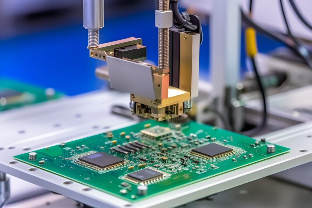
Why do different circuit boards have different solder mask colors?
PCB solder mask can be displayed in different colors, including green, white, blue, black, red, yellow, matte color, purple, chrysanthemum, bright green, matte black, matte green, etc. Under normal circumstances, white is used to make white PCB circuit boards for products such as LED lighting. Other colors are mostly due to product grading systems. Different companies have different colors. Some use red to indicate experimental boards, some use blue to indicate key boards, and some use black to indicate boards used inside computers.
Why is green oil widely used in PCB solder mask ink?
1. From the functional point of view, the ingredients added to green ink have been fixed for a long time. Basically, the equipment solution is for green, which is easy to develop and not easy to fall off.
2. For appearance inspection, it is obvious in contrast with the copper surface (yellow), and it is easier to detect defects such as scratches and offsets. Other miscellaneous oils are added with some powder substances that change the color. It is relatively costly for PCB production. But for the finished product, some colors look more high-end than green.
In addition, there is manual visual inspection in the PCB quality inspection process of the circuit board factory. For PCB manufacturers, green is more eye-friendly and more friendly to visual inspection staff.
3. Green ink can achieve smaller errors, smaller areas, and higher precision. Green, red, and blue have higher design precision than other colors.
4. Green ink has better characteristics than other colors. The green system has better characteristics than other colors, especially the plugging characteristics of green.
5. Green ink is relatively cheaper. Since green is the mainstream in the production process, and the process is the most mature and simple, the purchase volume of green ink will naturally be larger, so its purchase cost will be lower than other colors.
6. In order to reduce costs, many PCB ink manufacturers will also produce green oil in large quantities, which also makes the price of green oil lower.
7. In PCB processing, electronic product production includes board making and SMT patch. During this period, several processes must pass through the yellow light room, and the visual effect of green PCB boards in the yellow light room is the best.
8. In SMT patch processing, tinning, patch and AOI verification steps all require optical positioning calibration, and the green base plate is more friendly when identified by instruments.
9. Green PCB is also more environmentally friendly. When waste boards are recycled at high temperature, no toxic gases are released.
10. Other PCB colors, such as blue and black, are doped with cobalt and carbon respectively. Because of their weak conductivity, there is a risk of short circuit. In addition, like black, purple, and blue lights, the color of the PCB substrate is too dark, which will increase the difficulty of inspection and maintenance of the motherboard, and the process is not easy to control.
Does the color of PCB solder mask affect the circuit board?
In fact, PCB ink has no effect on the finished circuit board. But it has a great impact on the semi-finished products. For example, there are matte green, solar green, dark green, light green, etc. in green. The color is a little different. If the color is too light, it is easy to see that the appearance of the board after the plugging process is not good. If the color is too dark, the quality of the ink used by some circuit board factories is not good enough, and the ratio of resin and dye is problematic, bubbles will appear, and serious problems will fall off the ink during the final curing.
Why do PCB circuit boards need solder mask?
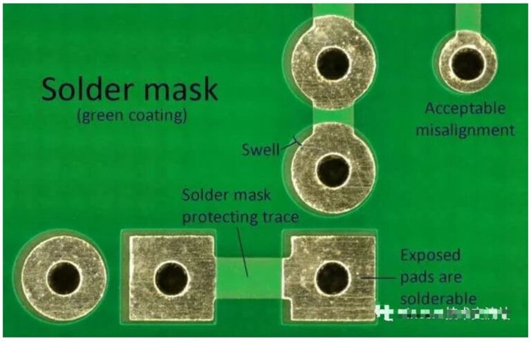
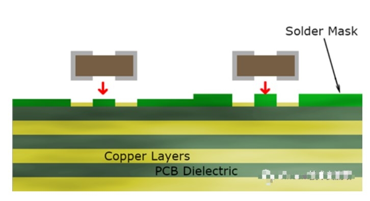
In the process of printed circuit board (PCB) processing and manufacturing, the coating of solder mask ink is a very critical process. The main function of solder mask on PCB is to protect the circuit, prevent conductors from being tinned; prevent electrical short circuits between conductors caused by moisture or chemicals; prevent short circuits caused by poor handling during the subsequent production and electrical installation of PCB boards; and prevent various harsh environments from invading PCB boards.
There are copper layers on both sides of the circuit board. PCB boards without solder mask are easily oxidized when exposed to the air, and become defective products, which also affects the electrical performance of the PCB board. Therefore, there must be a protective coating on the surface of the PCB circuit board to prevent the PCB from oxidizing with the air, and this coating is the solder mask covered with solder mask paint. Various colors of solder mask paint have also emerged, forming colorful PCB circuit boards, and the color of the solder mask has nothing to do with the quality and electrical performance of the PCB board.
The surface of the PCB needs to be soldered with electronic components, so part of the copper layer needs to be exposed to facilitate soldering of components. This part of the copper layer is the pad. As mentioned above, the exposed copper layer is prone to oxidation, so the pad also needs a protective layer to prevent oxidation; therefore, the pad is sprayed, which is what we often call PCB surface treatment. It can be plated with inert metals such as gold or silver, or a special chemical film to prevent the copper layer of the pad from being exposed to the air and oxidized.
PCB solder mask thickness standard
The PCB solder mask must have good film-forming properties, and its thickness is subject to regulatory requirements. Currently, most circuit board manufacturers conduct identification based on the US civil standard IPC-SM-840C. In this standard, the solder mask thickness of Class 1 products is unlimited; the minimum solder mask thickness of Class 2 products is 10um; the minimum thickness of Class 3 products should be 18um. The flame retardancy of the solder mask is usually based on the specifications of the US UL agency and must pass the requirements of UL94V-0 (UL94-flammability test of plastics used in components of devices and equipment).
PCB ink solder mask bridge
1. What is a solder bridge?
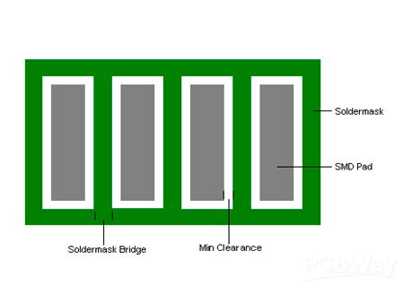
The solder bridge is the green oil between one window of the component pad and another window. It generally refers to the solder strips between the pads of the densely packed IC pins. The function of the solder bridge is to prevent the solder from flowing during welding and to prevent the device from short-circuiting. Usually, in order to prevent short-circuiting, the solder bridge of the pad must be guaranteed.
2. PCB solder bridge process
The process capability of the solder bridge is related to the ink color and copper thickness. The solder bridge of green oil is easier to control than that of mixed color ink, and the solder bridge can be kept to a minimum. The thicker the copper, the larger the solder bridge needs to be. The solder bridge of thin copper is easier to control than that of thick copper. Factors affecting whether the solder bridge process can be processed: whether the IC pin spacing is sufficient, the ink color of the board, and the copper thickness.
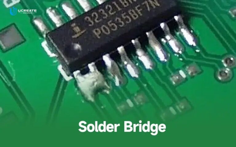
From the customer’s perspective, solder bridge processing has a high pass rate for finished products, better product quality, and beautiful appearance, but the price may be a little higher; from the manufacturer’s perspective, one is that it affects production efficiency and costs will increase. Usually, according to the acceptance standard IPC600-II, if the manufacturer does not specify the solder bridge, generally if it is a dense IC, the solder bridge will be made by default. If it is specified, We Ucreate factory will judge whether the solder bridge can be made based on the customer’s information and board requirements.
The process capability of solder mask bridge is not only related to the ink color and copper thickness, but also to the manufacturing capability of the PCB board factory. Solder mask bridge of green ink is easier to control than that of mixed color ink, and solder mask bridge can be kept to a minimum. The thicker the copper thickness, the larger the solder mask bridge needs to be. Solder mask bridge of thin copper is easier to control than that of thick copper.
a. When base copper ≤1OZ, solder bridge ≥3mil (green), 4mil (other colors). Some PCB manufacturers with good process technology can achieve 2.5mil for green and about 3mil for other colors. 8mil (only for solder bridge on the large copper surface of the whole board).
b. Base copper 2-4OZ, solder bridge ≥6mil; 8mil (only for solder bridge on the large copper surface of the whole board).
c. Between the tin-spraying surfaces in the large copper surface area, in order to prevent tin bridging, it is necessary to ensure that the tin bridge is ≥8mil;
PCB solder bridge DFM design
01. Solder bridge on substrate
The size of the solder bridge depends on the IC pad spacing of the circuit layer. If the IC pad spacing is too small, it is easy to cause tin short circuit when soldering devices. For example, taking green oil as an example, the IC pad spacing of the circuit is 8mil, and the pad opening is 2mil on one side, then the solder bridge is 4mil. In extreme cases, in order to keep the solder bridge, the IC pad spacing window can be opened on one side 1mil, so that even if the IC pad spacing is 6mil, a 4mil solder bridge can be made.
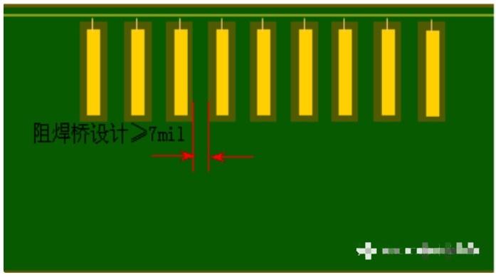
02. Solder bridge on copper foil
The IC pads on copper foil also need to have solder bridges. If there is no solder bridge on the IC pads on copper foil, the IC pads will be connected after the window is tinned, which is equivalent to connecting two IC pads into one pad. Although the pads on the copper surface are a network and will not cause a short circuit, the heat dissipation performance of the soldered components is poor, and it is not convenient to disassemble during repair.

Process interpretation of PCB solder mask layer
The solder mask exposure process in the printed circuit board is to cover the pads on the printed circuit board with a photographic base after screen printing, so that it is not exposed to ultraviolet rays during exposure. The solder mask protective layer is more firmly attached to the printed circuit board surface after ultraviolet light exposure, and the pads are not exposed to ultraviolet light, so that the copper pads can be exposed so that lead and tin can be applied on it during hot air leveling.
1. Pre-baking
The purpose of pre-baking is to evaporate the solvent contained in the ink and make the solder mask non-sticky. The pre-baking temperature and time are different for different inks. If the pre-baking temperature is too high or the drying time is too long, it will lead to poor development and reduce the resolution; if the pre-baking time is too short or the temperature is too low, the film will stick to the film during exposure, and the solder mask will be corroded by the sodium carbonate solution during development, causing the surface to lose gloss or the solder mask to expand and fall off.
2. Exposure
Exposure is the key to the entire process. If over-exposure occurs, due to the scattering of light, the solder mask at the edge of the pattern or line reacts with light (mainly the photosensitive polymer contained in the solder mask reacts with light), generating a residual film, which reduces the resolution, causing the developed pattern to become smaller and the lines to become thinner; if the exposure is insufficient, the result is the opposite of the above situation, and the developed pattern becomes larger and the lines become thicker. This situation can be reflected by testing: if the exposure time is long, the measured line width is a negative tolerance; if the exposure time is short, the measured line width is a positive tolerance. In the actual process, a “light energy integrator” can be used to determine the optimal exposure time.
3. Ink viscosity adjustment
The viscosity of liquid photosensitive solder resist ink is mainly controlled by the ratio of hardener to main agent and the amount of diluent added. If the amount of hardener added is insufficient, an imbalance in the ink properties may occur.
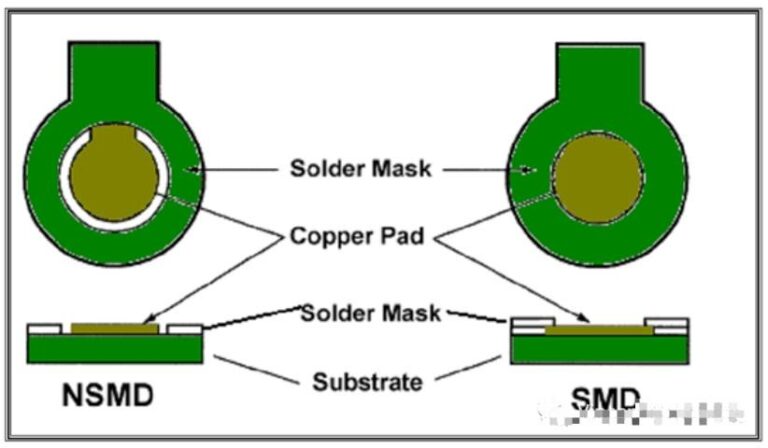
What is the reason for the PCB solder mask green oil to fall off?
1. When printing ink on PCB, the pre-treatment is not done properly, such as stains, dust or impurities on the surface of the PCB board, or some areas are oxidized. In fact, it is very simple to solve this problem. Just do the pre-treatment again, but try to clean the stains, impurities or oxide layer on the surface of the circuit board.
2. The baking time of the circuit board is short or the temperature is not enough, because the circuit board must be baked at high temperature after printing the thermosetting ink, and if the baking temperature or time is insufficient, it will cause the strength of the board ink.
3. The ink quality problem or the ink is expired, or the purchase of unknown brand ink, this will also cause the circuit board ink to fall when passing through the tin furnace.
PCB solder mask process quality acceptance standard
This standard applies to process monitoring and product monitoring of product quality during or after the solder mask process of the circuit board.
Alignment requirements:
1. Upper pad: The minimum solderable ring of the ink upper pad of the component hole cannot be less than 0.05mm; the ink upper pad of the via hole cannot exceed 1/2 of the single-side solder ring; the ink on the SMT cannot exceed 1/5 of the total pad.
2. No exposed lines: No copper is exposed at the adjacent pad and line due to offset.
Requirements in the hole:
1. Ink is not allowed to enter the component hole.
2. The number of ink entering the via hole is not allowed to exceed 5% of the number of via holes (under design guarantee).
3. The finished product aperture is greater than or equal to 0.7mm and the via hole that requires solder mask coverage is not allowed to have ink plugging.
4. If the wire holes are required to be plugged, there shall be no poor plugging (white light transmission) or ink overflow.
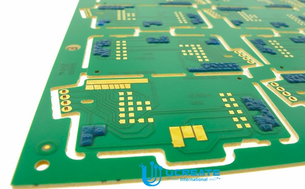
Surface requirements:
1. Ink accumulation, wrinkling, and cracking are not allowed on the ink surface.
2. Ink bubbling or poor ink bonding is not allowed (3M tape test failed).
3. No obvious exposure (spotting) is allowed on the ink surface. Local inconspicuous imprints do not exceed 5% of the board area on each side.
4. Copper exposure is not allowed on both sides of parallel lines. Obvious ink unevenness is not allowed.
5. Scratches on the ink surface are not allowed to expose copper, and fingerprints and missed printing are not allowed.
6. Ink scratches: The length and width are not allowed to exceed 5mm x 0.5mm.
7. Inconsistent ink colors on both sides are allowed.
8. If the surface mounting pad spacing is greater than 10mil and the green oil bridge width (design) is greater than 4.0mil, the green oil bridge is not allowed to break. If the solder mask process is abnormal and cannot meet the above requirements, the following conditions are acceptable: the number of green oil bridge breaks in each row is within 9%.
9. The diameter of the star point copper exposure point should be less than 0.1mm, and no more than 2 points on each side. No batch of exposed copper at positioning points is allowed.
10. No obvious screen printing and ink garbage particles are allowed on the surface.
Gold finger requirements:
1. Ink is not allowed on gold fingers.
2. Green oil is not allowed to remain between gold fingers.
Line surface requirements:
1. Copper layer oxidation and fingerprints are not allowed under ink.
2. The following ink conditions are not allowed:
① The diameter of the debris under the ink is greater than 0.25mm.
② The debris under the ink reduces the line spacing by 50%.
③ The debris under the ink is more than 3 points on each side.
④ The conductive debris under the ink crosses two wires.
3. Red lines are not allowed.
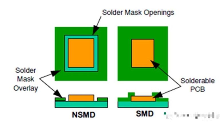
BGA area requirements:
1. No ink is allowed on the BGA pad.
2. No debris or dirt that affects the solderability is allowed on the BGA pad.
3. The vias in the BGA area must be plugged. No light transmission or ink overflow is allowed, and the height after plugging should not exceed the horizontal plane of the BGA pad; the opening of the plugged via is not allowed to be red.
4. The via holes (vent holes) in the BGA area with a finished aperture greater than or equal to 0.8mm do not need to be plugged, but copper exposure at the opening is not allowed.
Inspection method:
First board inspection
1. Responsible unit: Operator conducts self-inspection, IPQC conducts first inspection
2. Inspection timing:
① At the beginning of each continuous production batch.
② When the engineering data is changed.
③ Replace the potion, after maintenance
④ When changing shifts
3. Inspection number: First board
4. Control method: Batch production can only be carried out after the first board inspection is qualified
5. Record: Record the first board inspection results in the “Daily Report of First Inspection Record of Process”
Sampling inspection
1. Inspection responsibility: IPQC
2. Inspection timing: After the first board inspection is qualified, random inspection is carried out.
3. Inspection number: Random sampling, when sampling, take the panel and bottom plate for inspection.
4. Control method:
① Severe defects: 0 defects are qualified.
② B minor defects: three minor defects are converted into one severe defect.
③ If the random inspection is qualified, the batch will be transferred. If it is unqualified, it will be reworked or reported to the screen printing team leader or director for processing. The screen printing process must find out the reasons for the unqualified and improve them before continuing production.
Seven advantages of PCB solder mask green oil plugging holes
At present, except for the component pin holes, mechanical holes, heat dissipation holes and test holes in various PCB through holes, other conductive holes (Via Hole) do not need to be exposed and require solder mask ink plugging holes. In particular, HDI high-density connection technology is becoming more and more intensive. There are more and more VIP holes and VBP holes in PCB boards used for packaging, and most of them require via plugging oil. So what are the benefits of using solder mask plugging holes?
Green oil plugging holes means plugging green oil into the vias, generally filling two-thirds of the part, and it is better to be opaque. Generally, if the vias are large, the size of the ink plugging holes is different according to the manufacturing capacity of the board factory. Generally, holes below 16mil can be plugged, and larger holes need to consider whether the board factory can plug them.
1. Plug holes can prevent possible short circuits caused by dense pitch devices (such as BGA). This is why the vias under BGA need to be plugged during the design process. Because there is no plugging, this case of short circuit has occurred.
2. Plug holes can prevent tin from penetrating the component surface from the via hole during wave soldering of the PCB, causing a short circuit; this is because there are no vias or the vias are plugged within the wave soldering design area (generally the soldering surface is 5mm or more).
3. Avoid flux residue in the via hole.
4. After the surface mounting and component assembly of the electronics factory are completed, the PCB must be vacuumed to form a negative pressure on the test machine before it is completed.
5. Prevent the surface solder paste from flowing into the hole, causing cold soldering and affecting mounting; this is most obvious in the heat dissipation pad plus via.
6. Prevent tin beads from popping out during wave soldering, causing a short circuit.
7. Plug holes will be helpful to the SMT patch process.

 English
 中文
中文


