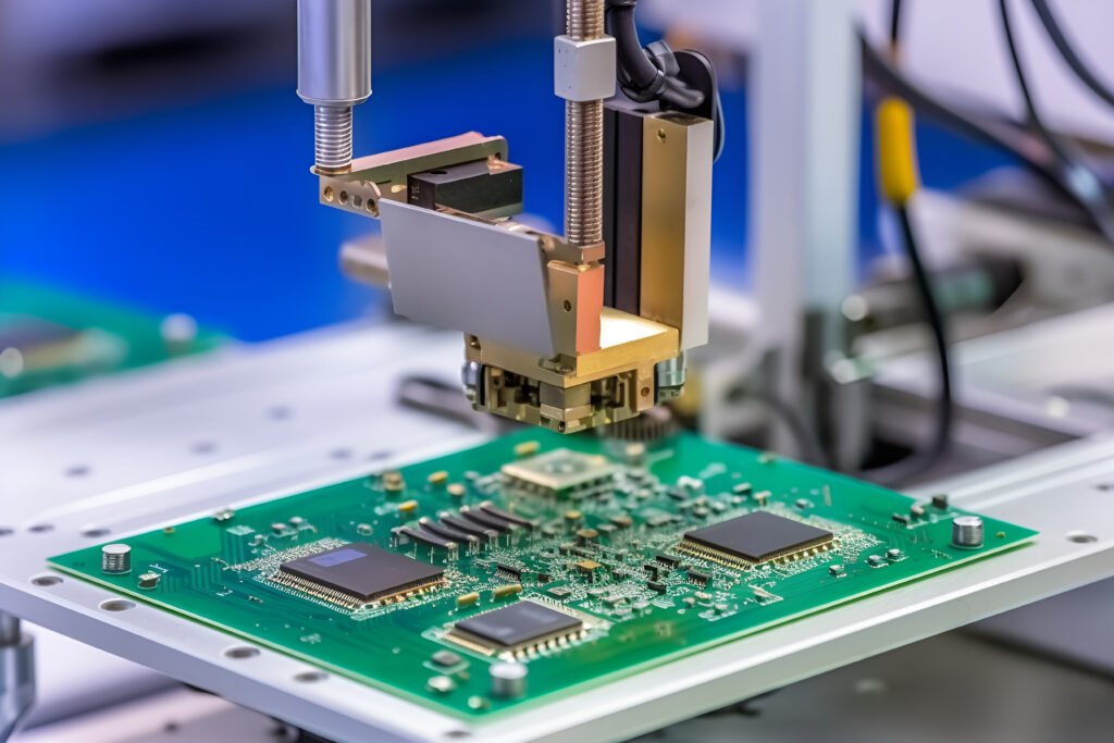
X-ray uses a cathode ray tube to generate high-energy electrons that collide with metal targets. During the collision, the electrons suddenly slow down, and the lost kinetic energy is released in the form of X-rays. For locations where the sample cannot be observed from the outside, the change in light intensity after X-rays penetrate materials of different densities can produce a contrast effect that can form an image, which can show the internal structure of the object to be tested, and thus observe problematic areas inside the object to be tested without destroying it.
What can PCB X-ray inspection do?
High-precision X-ray is an important method of non-destructive testing and a common method of failure analysis. Its main application areas are:
- Observe semiconductors, resistors, capacitors and other electronic components in different packages such as DIP, SOP, QFP, QFN, BGA, Flipchip, and small PCB printed circuit boards
- Observe the size, quantity, die stacking, and wire binding of the chip inside the device
- Observe chip cracks, uneven dispensing, broken wires, wire overlaps, internal bubbles and other packaging defects, as well as solder ball cold soldering, virtual soldering and other welding defects
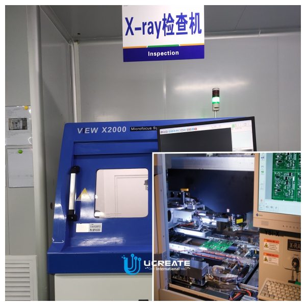
What are the advantages of PCB X-ray inspection?
The advantages of PCB X-ray inspection mainly include high detection coverage, strong penetration, production process evaluation ability, high cost performance, high detection accuracy, wide detection range, high detection efficiency, non-destructive detection, defect detection, three-dimensional imaging, automated processing, safety, and application in repair and maintenance.
- High detection coverage: It can detect a variety of problems such as cold solder joints, false solder joints, bridges, monuments, insufficient solder, pores, and device leakage, with a detection coverage of up to 97%.
- Strong penetration: It can penetrate the inside of the sample and perform imaging detection, such as poor cold solder joints and false solder joints, greatly shortening the detection time.
- Evaluation of production process: It can evaluate the production process, such as soldering thickness, soldering amount, etc.
- High cost performance: X-ray inspection systems have a high cost performance in the industrial field and have the performance of expensive products.
- High detection accuracy and high detection efficiency: It can provide a three-dimensional image of the inside of the PCB board, with higher detection accuracy and improved detection efficiency.
- Non-destructive detection: It can penetrate the circuit PCBs and chips without disassembling or damaging them, avoiding potential damage and costs.
- Defect Detection: Able to detect defects on PCBs, such as solder joint problems, open circuits, short circuits, defective components, lead gap problems, etc.
- 3D Imaging: Allows users to view and analyze the internal structure of PCBs and chips to gain a deeper understanding of the root cause of the problem.
- Automated Processing: Integrated with automated systems, large numbers of PCBs and chips can be processed automatically to improve production efficiency.
- Safety: Safe to operate, the amount of X-ray exposure used is much smaller than traditional technologies, and will not cause harm to the human body.
- Application in Repair and Maintenance: Used in the repair and maintenance of electronic equipment to help technicians find and solve problems.
We provide one-stop PCB solution, and we are a professional PCB manufacturer in China, from PCB manufacturing, component sourcing, to PCB assembly. At the same time, we provide a series of testing services, Manual Test, Microsectioning Test, X-ray inspection, PCB Electrical Testing, AOI Inspection, ICT, Flying Probe Test, Functional Circuit Test. To ensure that your electronic products meet the highest quality standards. We also offer free quotation after you send us the Gerber files.

 English
 中文
中文


