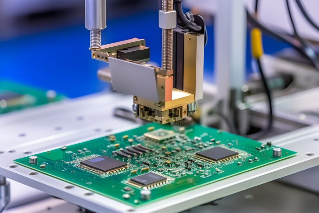
Currently, the typical process for processing printed circuit boards (PCBs) is the ‘graphic plating method’. That is, first in the outer layer of the board to be retained on the part of the copper foil, that is, the circuit of the graphic part of the pre-plated layer of lead and tin resist layer, and then chemically corrode the rest of the copper foil, known as etching. It is important to note that there are two layers of copper on the board at this point. In the outer layer etching process only one layer of copper must be completely etched away, the rest will form the final desired circuit. This type of graphic plating is characterised by the fact that the copper layer exists only underneath the lead-tin resist layer. Another process is that the entire board is plated with copper, and the portion of the board outside of the photographic film is simply tin or lead-tin resist. This process is called ‘full-plate copper plating’. Compared with the graphic plating, the biggest disadvantage of full-plate copper plating is that all parts of the board surface have to be plated with copper twice, and etching must also be etched off all of them. This creates a series of problems when the wire width is very fine. At the same time, side etching can seriously affect the uniformity of the line.
In the process of processing the outer circuit layer of a printed board, there is another method, which is to use a photographic film instead of a metal plating as a resist layer. This method is very close to the inner layer of the etching process, you can refer to the inner layer of the production process in the etching. Currently, tin or lead-tin is the most common resist used in the etching process with ammonia-based etchant. Ammonia etchants are commonly used chemical solutions that do not react chemically with tin or lead-tin. Ammonia etchant mainly refers to ammonia/ammonia chloride etching solution. In addition, ammonia/ammonia sulphate etching solution is also available in the market.
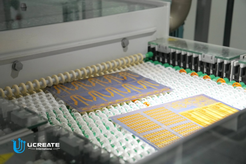
The sulphate-based etching solution can be reused because the copper in it can be separated by electrolysis after use. Because of its low corrosion rate, generally not seen in actual production, but is expected to be used in chlorine-free etching. Experiments have been made with sulphuric acid-hydrogen peroxide as an etchant to etch the outer graphics. For a number of reasons, including economic and waste disposal, this process has not yet been adopted on a commercial scale. Further, sulfuric acid – hydrogen peroxide, can not be used for lead and tin resist etching, and this process is not the main method of PCB outer layer production, so the majority of people rarely asked.
Etching quality and pre-existing problems
The basic requirement for etch quality is the ability to completely remove all copper layers except underneath the resist, and that’s about it. Strictly speaking, if it is to be defined precisely, the quality of the etching must include the consistency of the wire width and the degree of side etching. Due to the inherent characteristics of current etching solutions, which etch not only downward but also to the left and right directions, side-etching is almost unavoidable.
Lateral corrosion problem is often raised in the etching parameters to discuss one, it is defined as the side of the etching width and etching depth ratio, known as the etching factor. In the printed circuit industry, it varies over a wide range from 1:1 to 1:5. Obviously, a small side etch or a low etch factor is most satisfactory.
In many ways, the quality of the etching exists long before the printed board enters the etching machine. Because of the very close internal connections between the various processes or processes of printed circuit processing, there is no one process that is unaffected by and does not affect the other processes. Many of the problems identified with etch quality actually existed in the depatterned or even earlier processes. For the etching process of the outer layer of graphics, many of the problems end up being reflected in it because it represents a ‘reverse stream’ that is more prominent than in most printed board processes. At the same time, it is also because the etching is the last link in a long series of processes since the film, sensitisation, after which the outer layer of the graphics is transferred successfully. The more links, the greater the likelihood of problems. This can be seen as a very specific aspect of the printed circuit production process.
Theoretically speaking, printed circuits into the etching stage, in the graphic plating method of processing printed circuits in the process, the ideal state should be: plating of copper and tin or copper and lead and tin thickness should not exceed the sum of the thickness of plating-resistant photopolymer film, so that plating graphics are completely by the film on both sides of the ‘wall’ blocked and embedded in it. However, the reality of production, the world’s printed circuit boards after plating, plating graphics are much thicker than the photographic graphics. In the process of plating copper and lead-tin, problems arise when the height of the plated layer exceeds that of the photographic film and there is a tendency for it to build up horizontally. The tin or lead-tin resist layer covering the top of the line extends to both sides, forming a ‘rim’ that covers a small portion of the photographic film underneath the ‘rim’.
The ‘edge’ formed by tin or lead-tin makes it impossible to remove the photographic film completely during deposition, leaving a small amount of ‘residual adhesive’ underneath the ‘edge’ . ‘Residue’ or “residual film” left under the resist “edge” will cause incomplete etching. Line in the etching on both sides of the formation of ‘copper roots’, copper roots make the line spacing narrow, resulting in printed circuit boards do not meet the requirements of the party, and may even be rejected. As a result of the rejection will make the PCB production costs increased significantly. In addition, in many cases, due to the reaction and the formation of dissolution, in the printed circuit industry, the residual film and copper may also be formed in the corrosion of the liquid build-up and blocked in the corrosion machine nozzles and acid pumps, and had to shut down to deal with the cleaning, which affects the efficiency of the work.
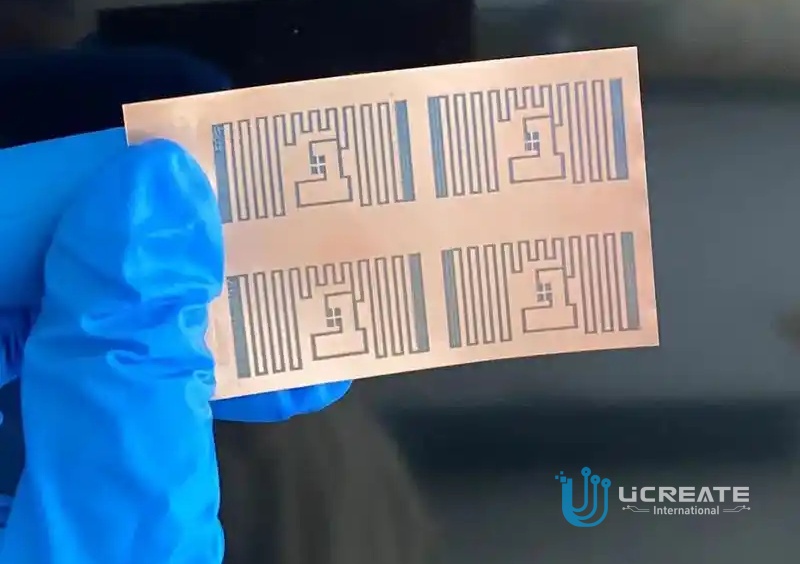
Equipment adjustment and interaction with corrosive solutions
Ammonia etching is one of the more delicate and complex chemical reaction processes in printed circuit processing. On the flip side it is an easy job to perform. Once the process is adjusted through, it can be continuous production. The key is that once the machine is switched on, it needs to be kept in a continuous working condition, and should not be stopped and dried. Etching process in a great degree depends on the good working condition of the equipment. For the time being, no matter what kind of etching solution, must use high-pressure spray, and in order to get a more neat line side and high quality etching effect, must strictly select the structure of the nozzle and spray method.

 English
 中文
中文


