
 English
 中文
中文Why is PCB testing so important?
During the PCB manufacturing process, micron-level defects may cause circuit short circuits, circuit breaks, or performance degradation. Modern electronic products have extremely high requirements for PCB reliability, and traditional manual visual inspection can no longer meet the inspection needs of high-density, miniaturized PCBs. Automated optical inspection (AOI) and X-Ray inspection have become the core links to ensure quality, which can accurately identify surface and internal defects and ensure product yield.
AOI inspection: using "eyes" to capture surface defects
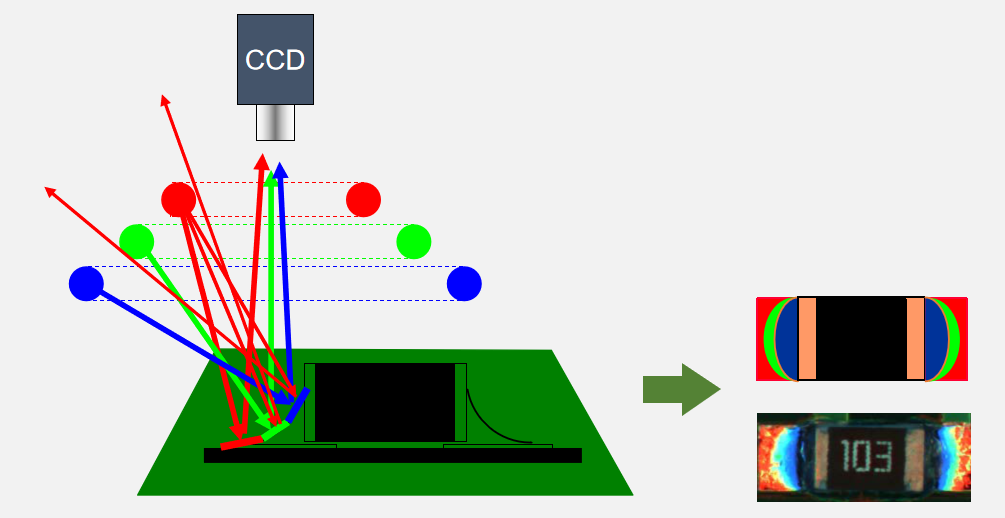
1. Working Principle
AOI uses a high-speed camera to scan the PCB surface, and combines light source systems such as ring light and coaxial light to highlight features such as solder joints and traces. It then uses algorithms to compare design files and identify anomalies in real time.
2. Core testing capabilities
- Solder joint quality: Identify problems such as cold solder joints, bridging, insufficient solder, and pad offset.
- Component placement: Detect missing components, incorrect polarity, offset, or rotation.
- Trace integrity: Detect breaks, shorts, or missing copper foil.
3. Advantages and limitations
- Advantages: fast detection speed, low cost, can locate defect coordinates, suitable for surface defect screening in large-scale production.
- Limitations: Unable to detect internal defects (such as BGA voids), relies on surface reflective properties, and has limited ability to identify complex three-dimensional structures.
4. Typical application scenarios
It is suitable for initial inspection of solder joints after SMT placement, quality screening of component placement and re-inspection of surface defects after DIP soldering, covering the key surface links of PCB manufacturing.
X-Ray inspection: "X-ray machine" that sees through PCB
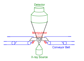
1. Working Principle
X-Ray uses high-frequency electromagnetic waves to penetrate PCBs, captures the attenuation signals of materials of different densities through detectors, generates images of internal structures, and can identify micron-level internal defects.
2. Core testing capabilities
- BGA/CSP solder joints: detect invisible defects such as voids, cold solder joints, and bridges.
- Inner layer of multilayer board: It is found that the through hole is not penetrated, the inner layer is short-circuited or open-circuited.
- IC packaging: Identify hidden problems such as chip cracks and bond wire breaks.
3. Technology upgrade direction
- 3D imaging technology: layered scanning generates a three-dimensional model to accurately locate the defect.
- Automatic defect classification: Different types of defects such as pores and slag inclusions are distinguished through algorithms.
4. Advantages and limitations
- Advantages: Non-destructive detection of internal defects, support for high-density packaging quality inspection, suitable for analysis of invisible solder joints and complex structures.
- Limitations: The detection speed is slow, the equipment cost is high, and it is more suitable for targeted detection of key processes or high-risk components.
5. Typical application scenarios
It is used for quality inspection of invisible solder joints such as BGA/QFN, verification of inner layer structures of high-layer PCBs and failure analysis, making up for the shortcomings of AOI in internal defect detection.
Collaborative inspection strategy of AOI and X-Ray
1. Division of labor and collaboration model
AOI and X-Ray form a complementary inspection system in the PCB manufacturing process:
- Surface defect screening: AOI prioritizes surface problems after SMT and welding, and quickly removes obviously defective products.
- Internal defect re-inspection: X-Ray conducts sampling or targeted inspections on high-risk components (such as BGA and multi-layer board through-holes) to identify internal hidden dangers.
2. The value of joint testing
The combination of the two can cover the entire quality control process of PCB manufacturing: AOI efficiently handles large-scale surface inspection tasks, and X-Ray focuses on solving highly complex internal defect problems, reducing the risk of missed inspections and improving overall reliability.
Future trends: intelligence and full process coverage
- AI-enabled detection: Deep learning algorithms optimize detection accuracy, reduce false alarms, and automatically adjust parameters to suit different product types.
- Online real-time detection: Embed AOI/X-Ray into the production line to achieve “detection-feedback-adjustment” closed-loop control and shorten defect response time.
- Multi-technology integration: Combine infrared thermal imaging and X-Ray to simultaneously detect electrical performance and structural defects and improve comprehensive analysis capabilities.
Conclusion
AOI and X-Ray inspections are like “double insurance” for PCB quality: AOI efficiently captures surface defects, and X-Ray deeply sees through internal hidden dangers. As the complexity of electronic products increases, the coordinated application of the two will become a necessary means to improve yield and reduce costs, providing key technical support for high-reliability electronic manufacturing.


