Silkscreen printing has incomparable characteristics of other printing methods: rich color effect, strong texture; large special color or dot printing; extensive substrate; thick ink layer and adjustable; application of different inks (solvent, UV, water, etc.). These characteristics make silkscreen printing have a very wide range of applications and play a huge role in many fields.

In stainless steel and ordinary iron products using the principle of electric corrosion, through the template screen can be fast and convenient to print exquisite, clear, accurate and accurate images and text, increasingly widely used. In the printed circuit board, more application is the use of copper coated foil laminate. In addition to drilling, hole metallization and circuit electroplating, the double-sided production process is basically the same as that of the single-sided laminate plate.
Preparations
Copper clad foil laminate is rigid and flexible, rigid plate sold in square meters, flexible plate must be cut into a size easy to work. To be easy to operate in use, large laminate must be cut into easy working sizes with saws or cutting beds. Its cutting tool, as necessary, can be used by sawing or cutting bed.
The surface of copper foil laminate with stripping agent during hot pressing and oil or chips during cutting should be removed first before printing. The removal method is generally with the grinder or brush to do mechanical removal, which is very effective for the cleaning of the section, the residual debris on the cutting surface to the back of the printing will cause failure, so it must be thoroughly removed, if necessary to use degreasing, rust performance of the purification agent removal.
To make a double-sided laminate. When making the lines of the two sides of the laminate, if you want to connect the two sides of the circuit, it is necessary to drill in the connection, and plating copper on the hole wall (the metallization of the hole) to connect the current, drilling copper plating can be circuit printing.
Drilling is a main process in the circuit board production, traditional drilling is mechanical drilling, aperture is larger, the smallest aperture is only about 100 μ m, with modern electronic products increasingly to portable, miniaturization, high integration, high performance trend, put forward the increasing demand for circuit board miniaturization, is the key to improve the level of circuit board miniaturization is more and more narrow line width and different levels between smaller micro holes and blind hole, so mechanical drilling cannot meet the requirements, can do the high precision microporous processing technology is laser micro drilling.
For the quality requirements of drilling, the main attention should be paid to the drilling must be fine, and the copper foil bulge can not occur at the hole wall and both ends of the hole. There have been various studies on drilling methods, and a special drilling machine for printed circuit board has been invented. Due to the difference of the laminate and the drill bit, the drilling is generally drilled at a high speed of (2~8) 104 r/min. Because the laminate is generally a glass fiber cured with epoxy resin, the drill must be high hardness. Another surface treatment must be performed after drilling the boreholes.
The process for double-sided laminate. The method of plating copper on the hole wall is not electrolysis but chemistry. In this method, the drilling laminate is first immersed in the palladium salt solution, and then put into the reducing agent mixed with copper ion solution and formaldehyde solution. Due to the adsorption of palladium on hydrogen, the copper ions are reduced to metal copper and attached to the hole wall.
In the operation, it should be noted that the thickness of copper plating is generally about 1 μ m. Sometimes, in order to strengthen this layer of copper, two solutions of copper pyrophosphate and copper sulfate should be used for plating, and the coating thickness after plating can be increased to 20~30 μm. After the copper plating of the hole wall should be processed again, and the screen printing of the circuit board can be done.
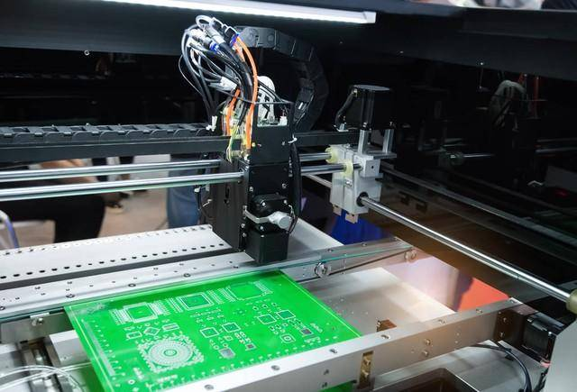
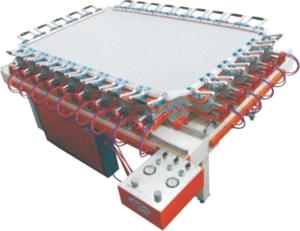
To correctly choose the screen, net frame, photosensitive materials, etc. The screen controls the fluidity of the ink, the printing thickness and determines the durability of the screen plate. Generally to choose high tension, single silk, flat woven polyester polyester wire mesh or stainless steel wire mesh. In addition, the new screen should be coarsened and degreased treatment, so as to ensure the quality of the screen version and prolong the service life of the screen. Network frame generally choose high tension aluminum mesh frame, the quality is ideal, we should pay attention to the control of network tension. The net frame of the stretched net should stay on the stretched net machine for more than 48h.
Reasonable control of network version tension should mainly pay attention to: (1) the consistency of the network version thickness, the uniformity of exposure, and the durability of the network version. (2) Accurately adjust and control the mesh spacing in the printing process, positioning and size stability, adjust the pressure of the scraper, the speed of the scraper, pay attention to the fluidity of ink, ink consumption and energy consumption. (3) Pay attention to the control of the factors affecting the tension, reasonable selection of bandage equipment and bandage method, printing photosensitive materials commonly used diazo photoreceptor, photosensitive diaphragm, etc. Diazo-type photosensitive emulsion is widely used in the production of screen printing screen plate. The sensitive diaphragm has the characteristics of uniform and controllable film thickness, high resolution, high definition, wear resistance, strong attachment and screen, and has been widely used in the character printing of printed board. Attention should be paid to grasp the thickness of the coating photosensitive film, generally printing resistance welding film to 25~30 μm is better, printed wires and characters to 15~20 μm is appropriate.
The designed circuit pattern is printed on the laminate to form an resist film, which is completed by screen printing. There are two cases of screen printing of resist film: (1) the circuit part is printed with resist ink, where the resist ink needs to retain the copper foil, so that in the corrosion, the line part is preserved, forming a conductive line. (2) do not resist corrosion ink printing circuit, on the contrary to print the part outside the circuit, that is, to make the part other than the printed circuit has corrosion resistance. When installing components, then plating solder, double-sided, multi-layer circuit boards are almost always printed using this method.
Electroplating to use solder or gold, electroplating soldering to use copper fluorororide electroplating liquid, the ratio of tin and lead in solder is 3 ∶ 2, the use of gold plating is weak acid solution. Plating corrosion resistant ink film must be able to withstand plating pretreatment solution and plating solution erosion, and finally must simply be able to peel off. Electroplating line, should be coated with copper into a certain thickness and then plated on it. Thickness of plating: 30 μm for copper, 10 μ m for solder, 7 μm for nickel bottom plating, and 25 μm for gold plating. After electroplating, the corrosion film is stripped, and the method is to remove with ink remover and soft brush.
Erosion ink commonly known as alkali soluble ink, screen printed circuit conductive pattern can withstand ferric chloride, acid copper chloride and other acid etching. The single copper foil laminate must immediately enter the screen printing corrosion ink process after the lower slope, brushing, cleaning and drying. Before screen printing, the corrosion ink should be stirred evenly, and generally no diluent should be used. The screen printing scraper is made of polyurethane rubber, the thickness is 8mm, shao hardness is about 7, the shape of the scraper is right Angle, the Angle of the scraper and the screen is 50~60, and the static distance between the screen and the substrate is 3~5mm, no matter the screen printing machine or manual operation, the film thickness of the corrosion ink drying should be properly controlled. If the film is too thick, it will affect the accuracy; the thin film will form the hole pinhole and increase the revision work. After screen printing, far infrared drying for 2min, and with natural drying method in 25~30, it takes 4h or longer, the hardness of the film forming pencil to reach 2H, the drying circuit board can enter the etching process, etching with 1~2%NaOH dilute lye spray off the film.
The corrosion resistance ink can also be prepared, the formula is as follows: rosin (industrial grade) 0.8~1kg, dark green or dark blue rubber plate ink 200g, Lide powder (32 mesh) 3kg, pine section, oil (industrial grade) 1000 ~ 1200 mL, stearic acid (industrial grade) 32g. When preparing, the rosin and stearic acid together heating melting, melting must leave the heater and then slowly add turpentine, pouring while stirring, do not make the rosin resetting, solid, and then add ink to dissolve it, finally, add lide powder fully stir or crush evenly. When preparing, the number of lide powder must be strictly selected. Do not use water bath method to avoid water vapor entering the press and forming it.
The cleaned printed circuit board shall immediately print the welding film, and the method shall apply the welding ink to the printing board, but for different screen printing machines, the process parameters are different. Generally speaking, the printing speed is controlled at 100 ~ 150 mm/s, the screen printing pressure is 4.0~6.0kg/cm2, the scraper hardness is 65, the scraper angle is 65~70, the scraper number is 1~2 times / surface, and the net distance is 4~8mm. Clean the screen press shell and work surface before starting the screen printing. Before printing the first plate, clean the mesh with a rubber roller and test it several times with white paper. Generally every 2h, need to clean the table once. Before the formal net printing, it is necessary to test the printing plate, and check the quality of the printing plate (printing oil is uniform, uniform thickness, no bad oil or oil into the hole phenomenon, no garbage dust, etc.), the net printing plate, need to be placed on the plate frame, 10~15min before the oven pre-drying.
There are two types, each class can be divided into one group and two components.
(1) photosolid retention welding ink: photosolid retention welding ink, also known as ultraviolet curing ink, its screen printing process conditions and corrosion resistance printing material is basically the same. The thickness of the welding resistance film should be appropriate, and the hardness of the pencil should reach 6~7H. If the film surface adhesion indicates that the curing time is insufficient or the film layer is too thick, the curing time can be extended appropriately.
(2) thermosetting type resistance welding ink: thermosetting type resistance welding ink are single components abroad, the materials used in China are generally mostly two components, the use of the mass ratio of 100 ∶ 5 will be resistance welding ink and curing agent mixed and fully stirring, and then static 30~45min decolding can be used. The service duration of the hybrid resistance welding ink is 7 days, and the curing condition is 120 ± 5℃ for 10min. If using the far infrared drying channel 3~5min can cure the film.
In contrast, single component photosolid welding ink has many advantages, such as no solvent, less volatile; low toxicity, can improve the production operation environment; fast drying speed, adapt to automatic or semi-automatic pipeline operation. The biggest advantage is that the curing temperature is low, does not produce thermal reaction to the laminate, will not make the substrate size change and cause warping phenomenon. The adhesion and heat resistance of thermosetting resistance welding ink to the substrate is better than that of photosolid type, so the requirements of photofixing resistance welding ink for the printed circuit substrate are relatively strict.
Anti-electroplating ink, like anti-etching ink, is also a liquid dilute alkali dissolved ink, mainly used for the production of double-sided or multi-layer printed board outer circuit graphics. Its function is net printing negative line graphics, in the graphic electroplating block metal ions to form an electroplating layer on it, it can also be used as anti-etching ink.
Anti-electroplating ink is mainly divided into thermosetting type, photosetting type and liquid photosensitive type. The drying temperature of the thermosetting ink film layer is 80~100℃, the drying time is 8~10min, the hardness of the dried film layer pencil is about 2H, can withstand electroplating copper, tin lead alloy, nickel, gold plating and acid or alkaline etching liquid, suitable for the circuit board with line width and spacing of more than 0.25mm. Photofixed ink has the advantages of good screen printing performance, thick coating, and the average level of screen printing can reach the line width and spacing of 0.2mm, which is difficult to achieve with thermosetting ink, but due to the curing degree of photofixed ink and inconvenient to remove ink, it is difficult that photosolid ink is difficult to be widely used.
Liquid photosensitive resistant electroplating ink is developed to solve the fine wire map and a kind of ink (commonly known as wet film), it overcomes the thermosetting ink and dry film production process, suitable for the production of fine wire and ultrafine wire, the most fine wire width can be formed in 2.54mm between the two disc 4 (0.075mm) wire, can also be used in multilayer plate inner fine wire used as anti-etching ink.
Acid inks have ordinary acid inks and acid inks soluble in alkali. Ordinary acidic ink is characterized by a certain alkaline resistance, because the organic solvent should be used when removing, so special attention should be paid to the operation. The main problem is that the ink is easy to peel off, overlapping adhesion phenomenon, and it is difficult to remove the ink. The solution is not to make the oxidation of the pretreatment surface, machine, mechanical grinding, do not use resin containing grinding, agent; the substrate cooling before stacking; accelerate the corrosion speed. Acid ink soluble in alkali is characterized by effective electroplating when not using alkali, alkali can be used to remove the ink, it is mainly used for the corrosion of ferric chloride. The easy problems in the use are pinhole, serrations, ink removal difficulties and easy to produce alkali pollution. The main method to solve these problems is to avoid the use of dry ink, due to pinhole when too dry, can be added to dilute the ink or use larger mesh screen; after corrosion, quickly with alkali, heat alkali, increase the spray hydraulic; use 40~50% strong alkali, and then add about 10% lotion.
Whether the positioning method is correct and reasonable or not will directly affect the quality of screen printing. In order to ensure the accuracy of each web printing, it is necessary to adopt a strict positioning method. At present, the medial positioning method is widely used, as shown in the figure.

The inner positioning method is to select two points as the process positioning hole on the diagonal of the printed circuit board shape machining line. The spacing between the two points should be as large as possible, and it does not affect the electrical performance and appearance of the line. The aperture of the two holes is generally controlled at 0.8~1.0mm. The inner positioning method is suitable for either mechanical operation or manual screen printing. First, when the secondary net printing corrosion ink, the two process holes and circuit graphics are printed together. After the etching, the double head drill is used. If a single-head drilling machine is used, the operation hole position should be accurate, so as not to cause the distance between the two holes, resulting in inaccurate positioning. In the net printing resistance welding ink and positive and negative marking ink, with these two process holes positioning. In the machining of printed circuit boards, such as punching material, these two process holes should also be positioned.

 English
 中文
中文


