English
 中文
中文Currently, the standard package used to house various multi-functional semiconductor devices such as FPGAs and microprocessors is: BGA (Ball Grid Array).
Components in BGA packages are used in a wide range of embedded designs, either as host processors or as peripherals such as memory.
In HDI design and layout, the most difficult components to design and solder are BGAs with tall pins and small pin spacing.
BGA packages can be divided into standard BGA and micro BGA. The demand for I/O availability brings many difficulties, even for experienced PCB designers, especially in multi-layer circuit board. Here we mainly introduce BGA PCB design skills .
- Getting started with PCB layout using BGA
Since the BGA is often the main processor in a device and may need to interface with many other components on the board, it is common practice to place the largest BGA component first and use that to start the PCB layout.
Although it is not necessary to place the BGA first, the largest BGA will determine the number of layers and removal strategy you use in the routing tape assembly.
When starting PCB layout with a BGA, there are a few tasks you need to complete to ensure successful routing:
(1 )Number of signal layers
Determine the signals required for the stackup. The number of layers will affect the number of plane layers and the final trace width required to be routed into the design.
(2)Fan-out
How to enter and exit BGA? Need to control impedance? These questions will determine the number of layers in the stack and then determine how to route the inner layers.
There are also issues of design and qualification levels, with BGA high-reliability designs requiring product-specific reliability standards of Level 3/3A or higher.
For example some military aerospace specifications require pad sizes that will exceed the IPC-6012 Class 3 annular ring requirements, so a standard dog bone fan will no longer work due to tolerances, annular ring and solder mask requirements.
By taking some of these points into consideration early in the design process, it is now possible to use BGAs for PCB layout in three tasks.
2. BGA PCB design tip 1: Define a suitable exit path
The main challenge with BGA placement and routing is ensuring a suitable exit path for manufacturability (DFM) and not resulting in PCB rework after assembly.
For multi-layer BGAs, egress routing rules involve routing traces through multiple rows of pins. Some of these traces may carry high-speed signals and require proper spacing of traces to prevent crosstalk. Other signals may be slower configuration signals that can be routed more closely. Clustered together, there is less risk of crosstalk or excessive noise.
The example below shows BGA escaped routing on 2 inner layers. We can see that on these internal layers the traces are being routed to multiple rows of vias (more than two), which is appropriate since there are no routes to surface pins.
On the surface, it’s most common to just route to the outer two rows due to the pad size in the BGA pad pattern, the need for clearance, and the fan-out style (especially dogbone fan-out).

BGA routing is usually divided into four quadrants to facilitate routing
On the top layer, underneath the BGA, many of the pads in the land pattern need to be connected to vias so that they can be connected to the internal layers of the entire PCB.
For larger pitch BGAs (up to 1 mm), dogbone fan-out is the standard method for making these connections.
These small traces connected to the vias provide access to the outer two rows of pins on the surface layer (underneath the BGA), as well as the remaining internal pads via vias from the inner layer.

Standard dogbone fan-out for BGA routing and surface breakout
While dogbone fan-out is the standard method for coarse-pitch BGAs, vias in the pads give you more flexibility on the surface. As the pin pitch becomes smaller, the trace width required to reach each layer of BGA between pins becomes smaller and smaller.
For controlled impedance signals, this means you will need thinner laminates and ultimately HDI technology to ensure you can route to the BGA.
3. BGA PCB Design Tip 2: Grounding and Power
In a large BGA, it’s likely that multiple pins will be dedicated to ground and power. In some components, especially large processors that must support multiple high-speed digital interfaces, a large portion of the pins may be dedicated to power and ground. Additionally, the component may require multiple voltage levels, which means power from multiple sources needs to be routed to the board.
The easiest way to manage power connections in a BGA is to use power rails, usually on one or two plane layers. Placing power and ground on adjacent layers with thin dielectric layers will also help maintain power integrity by providing inter-layer capacitance.
We often talk about pushout or escape routes underneath the BGA, but these are not the only types of routes created near the BGA pins.
Connections to power rails, ground planes or polygons, and routing between pins may all need to be performed under the same BGA, meaning that in addition to polygons for power/ground on the same layer, you may also see pins Wiring between feet. You can see the example below:
Example routing on inner layer below BGA using pad vias. The polygon provides power to certain pins, while signal lines are routed to components outside the BGA.

Example routing on inner layer below BGA using pad vias. The polygon provides power to certain pins, while signal lines are routed to components outside the BGA
Example routing on inner layer below BGA using pad vias. The polygon provides power to certain pins, while signal lines are routed to components outside the BGA
4. BGA PCB Design Tip 3: Determine PCB Layer Stack
The BGA pinout and number of I/Os on the BGA can be used to determine the number of layers required for the PCB stackup. Once the PCB Layout engineer determines the trace width required to route controlled impedance lines to the BGA, the maintaining impedance can be determined Required layer thickness. Add to this the number of rows in the BGA and you can calculate the total number of signal layers required for the PCB stackup.
Typically, no vias are required on the outside of the first two rows of a BGA device, so routing can be done on the surface layer. This is the case with dogbone fan-out, via-in-pad, or alternative fan-out, and the pattern can then be repeated throughout the BGA to determine the total number of layers required for the fan-out signal.
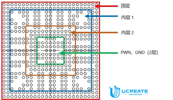
GND pins are typically staggered between signal pins, and GND should be staggered between signal layers to provide isolation where needed. The figure below shows how to count the number of rows in a BGA to determine the number of signal layers required.
In the example below, a flip-chip BGA is shown with some pins removed from the internal rows. Since some of these pins have been removed, signals can be routed there and to these internal pins, so more than 2 rows can be accessed from the internal layer.
The main internal squares of this particular BGA are probably for power and ground, requiring at least double sided PCB. With these layers and the backside layer, the total number of layers required to fully fan out and route this BGA will be at least 6 layers.