
 English
 中文
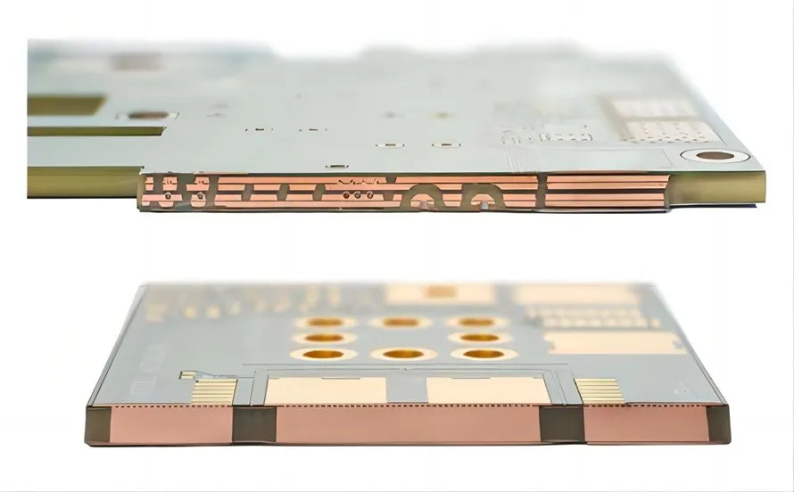
中文In the standard PCB production process, the thickness of the copper foil is usually based on the application requirements, but when the thickness of the copper foil is greater than or equal to 2 ounces (i.e., ≥ 2oz, equal to 0.71mm), this PCB is known as a thick copper PCB, which, by virtue of the ultra-high thickness of the copper layer, is able to carry more current, and at the same time, has excellent heat dissipation performance, which is widely used in high-power power supplies, industrial control, communications base stations, and other areas .The PCB is widely used in high-power power supply, industrial control, communication base station and other fields.However, its production process faces a number of serious challenges.
I. Material selection challenges
Thick copper PCB on the material requirements, need to take into account the electrical conductivity, thermal conductivity and mechanical properties, which makes the choice of materials is extremely complex.Like copper, brass and other high conductivity, high thermal conductivity materials meet the requirements, but the price is high, significantly increasing production costs.Moreover, these materials are difficult to process, the processing technology and equipment requirements are harsh, in the actual production need to carefully weigh the cost and performance, choose the appropriate material.
II. Manufacturing process dilemma
The manufacturing process of thick copper PCB is more complex than that of ordinary PCB, which needs to go through several processes, such as opening, drilling, plating, etching and so on.
In the manufacturing process, you need to ensure the uniformity and thickness of the copper layer, but also to control the parameters of each process to ensure product quality and stability.
Etchinglink: thick copper PCB etching process difficulty is far more than ordinary PCB, with the increase in copper thickness, the side of the etching problem is more and more serious, affecting the line accuracy and stability.In order to solve this problem, we need to use differential etching technology, and reasonably adjust the etching parameters, but because of the wide range of copper thickness changes, the precise control parameters are extremely difficult, and the stability of the process is a huge challenge.
Drillinglink: thick copper PCB is prone to hole wall roughness, pad cracking and other issues.This is caused by the physical properties of the thick copper layer and the interaction between the drill bit and the material, need to optimise the drilling process, adjust the parameters of the equipment to improve, but the effect is limited.
Lamination: the presence of copper layer affects the flow of resin and interlayer bonding, to strictly control the rate of heating, pressure and other parameters, a little carelessness will lead to poor lamination, affecting the final quality of the product.
III. Heat treatment complexity
Heat treatment is an important part of the production process for thick copper PCBs, with the aim of eliminating internal stresses and improving overall performance.However, the process is affected by a variety of factors, and a slight deviation in temperature, time, cooling method and other parameters may lead to changes in material properties and affect product quality.Precise control of these parameters to ensure product stability and quality consistency is the main challenge facing the heat treatment stage.
IV. Welding reliability issues
The soldering of thick copper PCBs is extremely difficult.Due to the high copper content, special soldering materials and processes are required to ensure reliable soldering quality.During the soldering process, the slightest lack of attention may result in soldering defects that affect the stability and electrical performance of the circuit connection, which in turn affects the realisation of the function of the entire PCB in the electronic device.
V. Reliability test pressure
Thick copper PCBs are subjected to rigorous reliability tests that cover a wide range of indicators such as voltage withstand, insulation resistance, and weather resistance.These tests not only need to comply with strict standards, but must also be conducted under diverse environmental conditions to fully simulate actual use scenarios.This undoubtedly increases the complexity and difficulty of testing, and places extremely high demands on product quality and stability.
With its excellent current-carrying and heat dissipation properties, thick copper PCBs occupy an important position in high-power electronic devices.However, the production process of thick copper PCBs faces many difficulties, from material selection, manufacturing process to heat treatment, from soldering reliability to reliability testing, each link is full of challenges.These difficulties not only put forward extremely high requirements on the technical level of PCB manufacturers, but also challenge the fine management of the production process.With the continuous development of science and technology and the growing demand for high-performance PCBs for electronic equipment, overcoming the difficulties in the production of thick copper PCBs and improving the quality and performance of products will be an important direction in the field of electronics manufacturing that is constantly explored and pursued, and a key factor in promoting the upgrading and development of related industries.


