
 English
 中文
中文Double-sided printed circuit boards have gained popularity in modern electronics due to their versatility and compact design. In this comprehensive guide, we will delve into the intricacies of 2 layer PCB board designs, explore their advantages and disadvantages, discuss specific design rules and guidelines, examine layer connection methods, and provide insights into testing and debugging techniques. Whether you’re a novice or an experienced PCB designer, this guide from Ucreate International will equip you with the knowledge to confidently handle double-sided PCB projects.
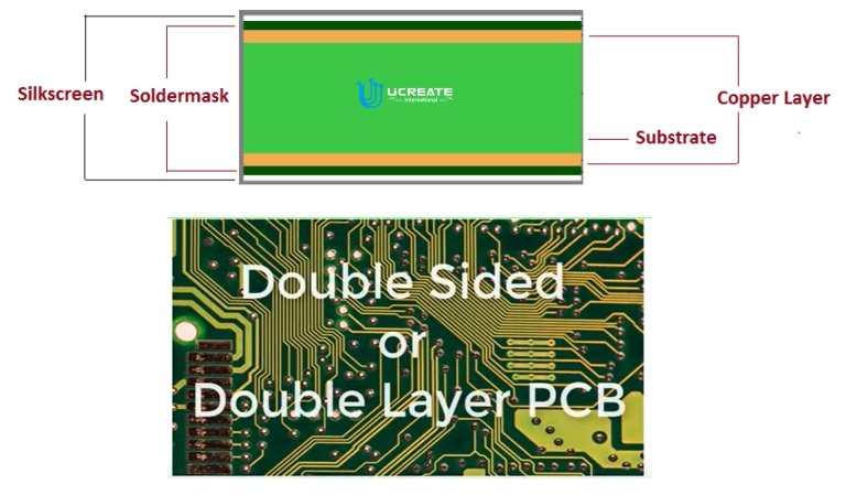
What is a double-sided PCB?
A double-sided PCB, also known as a double layer PCB, is a type of printed circuit board that incorporates conductive traces and components on both the top and bottom layers. Unlike single-sided PCBs that have components and traces on only one side, two-layer PCBs offer increased flexibility and design possibilities. By utilizing both sides of the board, designers can achieve higher component density, optimize space utilization, and accommodate more complex circuitry.
The construction of a double layer pcb board involves sandwiching a non-conductive substrate, typically made of fiberglass-reinforced epoxy, between two copper layers. These copper layers are etched to create the desired circuitry pattern, which includes signal traces, power planes, ground planes, and component pads. The traces on the top layer are interconnected with those on the bottom layer through vias, which are conductive holes drilled through the board. Vias provide electrical connections between the layers, allowing for the flow of signals and power.
Advantages and disadvantages of using PCBs with top and bottom layers
Advantages:
1. Increased component density and reduced PCB size
By utilizing both sides of the board, double sided circuit boards allow for a higher component density. This means more components can be placed on a smaller board, making it ideal for compact electronic devices where space is limited.
2. Enhanced routing options and flexibility
With conductive traces on both sides, designers have more routing options available to them. This flexibility enables efficient and optimized trace routing, leading to better signal flow and reduced signal interference.
3. Improved signal integrity and reduced noise interference
Separating the signal and ground planes on different layers helps improve signal integrity by reducing noise interference. This is particularly important for high-frequency signals and sensitive circuitry, where maintaining signal integrity is crucial for overall performance.
4. Cost-effective compared to multilayer PCBs
Double-sided printed circuit boards are generally more cost-effective than multilayer PCBs. They require fewer layers and manufacturing processes, resulting in lower production costs. This makes them an attractive option for projects with budget constraints.
5. Ease of assembly and maintenance
Double copper layer PCBs are relatively easy to assemble and maintain. With components mounted on both sides, accessibility for soldering and rework is simplified. Additionally, troubleshooting and debugging become more manageable due to the clear separation of circuitry on different layers.
Disadvantages:
1. Limited routing space compared to multilayer PCBs
2 Layer PCBs have less routing space compared to multilayer PCBs. This can be a challenge when designing high-density circuits with a large number of components and complex interconnections. Careful planning and optimization are necessary to ensure efficient use of available routing space.
2. Increased complexity in design and layout
Designing double-sided circuit boards can be more complex compared to single-sided PCBs. The placement of components and routing of traces on both sides require careful consideration to avoid conflicts, ensure signal integrity, and minimize crosstalk. This complexity may increase the design and layout time, especially for intricate and densely populated circuits.
3. Potential for signal crosstalk and interference between layers
With traces on both sides of the board, there is a potential for signal crosstalk and interference between layers. Crosstalk occurs when signals from one trace interfere with adjacent traces, leading to signal degradation and reduced performance. Proper design techniques, such as trace separation, ground plane placement, and signal routing considerations, are necessary to mitigate these issues.
4. Limited thermal dissipation capabilities compared to multilayer PCBs
Two-layered printed circuit boards have less effective thermal dissipation compared to multilayer PCBs with dedicated internal power and ground planes. The limited space available for heat sinks and thermal vias can lead to higher operating temperatures, potentially affecting the performance and reliability of heat-sensitive components. Thermal management techniques, such as adding heat sinks, optimizing component placement, and using thermal vias, are essential to address these thermal challenges.
While these disadvantages exist, they can be overcome with careful planning, design optimization, and adherence to best practices. Top and bottom copper layer PCBs remain a popular choice due to their versatility, cost-effectiveness, and suitability for a wide range of electronic applications.
Design Rules and Guidelines for 2-Layers PCBs
1. Component placement and clearance
Careful component placement is crucial to avoid conflicts and interference between components on different layers. Ensure sufficient clearance between components, especially taller components, to prevent short circuits or mechanical interference.
2. Trace routing techniques
Proper trace routing is essential to maintain signal integrity and minimize noise. Use techniques such as avoiding sharp corners, maintaining consistent trace widths, and minimizing trace lengths to reduce signal degradation and interference. Follow specific design guidelines for high-speed signals and impedance control.
3. Ground plane placement
Ground planes play a vital role in reducing noise and providing EMI shielding. Ensure proper placement of ground planes on both sides of the PCB to create a low-impedance return path for signals and reduce electromagnetic interference (EMI). Connect ground planes with vias to establish a solid ground plane throughout the PCB.
4. Via placement and optimization
Vias are crucial for layer connectivity and signal routing in PCBs with top and bottom layers. Place vias strategically to minimize signal crosstalk and interference. Optimize via placement for efficient layer connectivity while considering signal integrity, thermal management, and manufacturability.
5. Thermal management and heat dissipation
Two-layer PCB may have limited thermal dissipation capabilities compared to multilayer PCBs. Consider thermal management strategies such as adding heat sinks, thermal vias, and utilizing copper pours for heat dissipation. Optimize component placement to facilitate airflow and minimize heat concentration.
Please note that specific design rules and guidelines may vary based on your project’s requirements, circuit complexity, and the capabilities of your chosen PCB manufacturing process. At Ucreate International, we offer a comprehensive one-stop service, providing double sided pcb board prototype and rigid & flex double layer pcb assembly service ,handling.
How are the layers connected in a double-sided PCB?
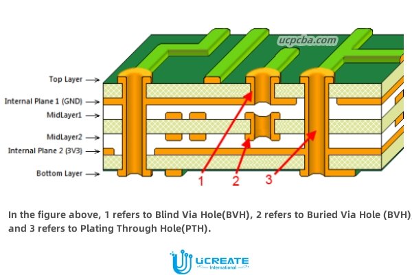
In a double-sided printed circuit board, the layers are connected by vias, which are conductive paths that allow electrical connection between the top and bottom layers of the board. Via holes are typically created by drilling holes in a PCB and then coating the inside of the hole with a conductive material, such as copper. Vias provide paths for signals and power through different layers of a PCB.
Ucreate International’s production department uses different types of vias in double-sided PCB prototype and volume pcb board prodcuts.
1 . Through-hole vias
These are the most common type of vias and extend from the top layer to the bottom layer of the PCB, connecting all layers in between. Through-hole vias are drilled through the entire thickness of the board.
2. Blind vias
These vias connect one or more inner layers of the PCB to the top or bottom layer, but they do not extend through the entire board. Blind vias are drilled from the outer layer and stop at a specific depth within the board.
3. Buried vias
Unlike through-hole and blind vias, buried vias do not extend to the outer layers of the PCB. They connect multiple inner layers without reaching the top or bottom layer. Buried vias are drilled and filled with conductive material, allowing connections between inner layers while maintaining signal integrity on the outer layers.
The placement and optimization of vias are critical for efficient layer connectivity in a double-sided PCB. Careful consideration is given to the location, size, and density of vias to minimize signal interference, ensure proper signal routing, and optimize the overall performance of the circuit.
It’s worth noting that the specific type and use of vias may vary depending on the complexity and requirements of the PCB design, as well as the manufacturing capabilities and constraints. Designers and engineers work closely to determine the appropriate via strategy that meets the electrical and mechanical requirements of the double-sided PCB design.
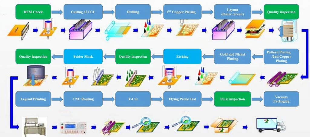
Two sided printed circuit boards manufacturing as below:
1. Visual Inspection
Perform a thorough visual inspection of the PCB to check for any soldering defects, component placement accuracy, and potential physical damage. Look for any missing or misaligned components, solder bridges, or damaged traces.
2. Continuity Testing
Use a multimeter or continuity tester to verify electrical connections and trace integrity. Check for proper continuity between different points on the PCB, including component pins, vias, and traces. This helps identify any open circuits, short circuits, or faulty connections.
3. Functional Testing
Conduct functional testing to verify the overall functionality of the PCB. This can involve using specialized testing equipment, such as oscilloscopes, logic analyzers, or function generators, to stimulate and measure the response of various components and circuits. Test fixtures may be used to interface with the PCB and automate the testing process.
4. Signal Analysis and Waveform Measurements
Analyze the signals on different nodes and measure waveform characteristics to assess signal quality and integrity. This can involve checking for noise, distortion, or unexpected signal behavior. Use appropriate test equipment, such as oscilloscopes or spectrum analyzers, to capture and analyze signals.
5. Thermal Imaging
Use thermal imaging cameras or temperature sensors to identify potential hotspots on the PCB. This helps detect any thermal management issues or components that are operating at elevated temperatures. Proper thermal management is crucial for the reliability and performance of the PCB.
Throughout the testing and debugging process, it is important to document any identified issues, perform root cause analysis, and implement appropriate corrective measures. Repeat the testing process as necessary to ensure that all issues have been resolved and the PCB is functioning as intended.
Conclusion
It is crucial to master the design, advantages, connectivity, and testing of double-sided PCBs for the successful implementation of electronic projects. By understanding the design principles and following specific guidelines, designers can optimize the performance and manufacturability of double-sided circuit boards. Key considerations in the design process include proper component placement, trace routing techniques, ground plane placement, via optimization, and thermal management strategies.
Moreover, layer connectivity is established using various types of vias, including through-hole, blind, and buried vias. These vias create pathways for electrical connections, ensuring efficient connectivity between layers in dual-layer PCBs.
Testing and debugging are crucial steps in guaranteeing the functionality and reliability of dual-layer PCBs. To identify and resolve any issues or defects in the PCB, common techniques include visual inspection, continuity testing, functional testing, signal analysis, and thermal imaging.
Pls send mail to Sales@ucpcba.com with your PCB Gerber files or Bom list. Or you can submit online form directly, Pls confirm that you have filled in the correct email. If you have whatsapp please try to fill in, so that we can contact you as soon as possible, thanks!


