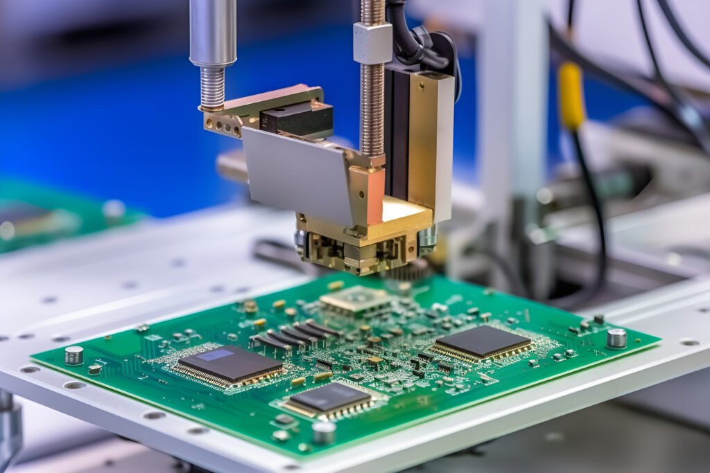
In the design of printed circuit boards (PCBs), the heart of modern electronics, an even number of layers has become the industry standard choice.This design preference is not accidental, but is based on a full range of considerations, from the manufacturing process to the final performance.In this article, we will systematically analyse the advantages of even-layer PCBs in terms of both manufacturing process and electrical performance.
I. Natural suitability of production processes
1. Optimisation of the basic manufacturing process
Even-layer PCBs fit perfectly into the standard PCB manufacturing process:
- Symmetric lamination process: all material layers can be combined in pairs.
- Improved drilling accuracy: symmetrical structure ensures uniform force during drilling.
- Etching consistency: symmetrical distribution of copper foils makes the etching process more stable.
2. Cost control advantages
Reduces production costs by 15-20% compared to odd-layer designs:
- Elimination of additional dielectric layer material
- Avoidance of special process steps
- Increase line utilisation
II. Innate strengths of the physical structure
1. Improved mechanical reliability
- Thermal stability: symmetrical structure enables uniform distribution of the coefficient of thermal expansion
- Deformation resistance: Effective reduction of the risk of plate buckling (typical value <0.7%)
- Structural strength: balanced stress distribution, life expectancy increased by 30% or more
2. Production yield guarantee
Actual production data shows:
- Yield of 6-layer board is 8-12% higher than 5-layer board.
- Yield of 8-layer board is 5-8% higher than that of 7-layer board.
- More accurate thickness tolerance control (within ±10%)
III. Excellence in electrical performance
1. Signal integrity guarantees
- Complete reference plane: each signal layer has an adjacent ground/power layer
- Impedance control accuracy: typical deviation <5% (~8-12% for odd layers)
- Crosstalk suppression: 3-5dB reduction in near-end crosstalk
2. Power integrity optimisation
- 20-30% lower supply loop inductance
- Flatter power supply impedance (1-100MHz range)
- Improved decoupling capacitor utilisation
IV. Flexible response to special scenarios
While the advantages of an even number of layers are obvious, engineers will consider an odd number of layers in the following situations:
- Ultra-low cost consumer electronics (e.g., disposable electronics)
- Ultra-high layer count PCBs (variance reduction at 12+ layers)
- Special mechanical constraints (e.g. shaped mounting space)
Professional advice
Recommended for new design projects:
- Even number of layers preferred for 4-12 layer boards
- High-speed circuits must use even layer design
- RF circuits are recommended to be ≥ 6 even layer structure
This design choice reflects the “optimal solution” way of thinking in the field of electronic engineering, by balancing process feasibility and performance requirements to ensure that electronic products work reliably in a variety of application environments.As circuit density continues to increase, the advantages of even-layer design will be more prominent.

 English
 中文
中文


