
 English
 中文
中文High Density Interconnect (HDI) printed circuit boards have revolutionised the electronics industry by enabling greater circuit density and miniaturisation. Ucreate International Design explores the basics of HDI PCB technology, highlights its key benefits, and addresses the challenges and considerations involved in HDI board design.

Understanding HDI PCB Technology
1. Introduction to High-Density Interconnect PCBs
High-Density Interconnect (HDI) PCBs are a type of printed circuit board that offers increased circuit density and miniaturization compared to traditional PCBs. They are designed to accommodate a higher number of components and connections in a smaller footprint. HDI PCBs utilize advanced manufacturing techniques and design methodologies to achieve these goals.
2. Key characteristics that differentiate HDI PCBs from traditional PCBs
Increased Circuit Density
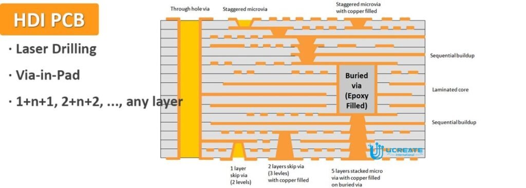
HDI PCBs excel at achieving higher circuit densities. They utilize various technologies such as microvias, blind vias, and buried vias to create a more complex and compact interconnection structure. These technologies allow for more routing channels, enabling more components to be placed on the board.
Miniaturization
One of the primary advantages of high-density printed circuit board is their ability to facilitate miniaturization. By reducing the size of vias and utilizing smaller components, HDI PCBs enable the creation of smaller and lighter electronic devices. This is especially crucial in industries such as consumer electronics, medical devices, and aerospace, where compact and lightweight designs are highly desirable.
Advanced Interconnection Technologies
HDI PCBs employ advanced interconnection technologies to optimize signal integrity and electrical performance. Microvias, which are small diameter vias, allow for shorter signal paths and reduced parasitic capacitance and inductance. This results in improved signal quality and higher data rates.
High-Frequency Capability
Due to their optimized signal integrity characteristics, HDI PCBs are well-suited for high-frequency applications. They can handle higher data transfer rates and support technologies such as RF (radio frequency) and microwave communication. This makes high-density Interconnect Board ideal for applications like wireless devices, telecommunications, and high-speed data transmission.
Design Flexibility
High-Density Circuit Board offer greater design flexibility compared to traditional PCBs. With the use of advanced design tools and manufacturing processes, designers can achieve intricate layouts, complex routing, and precise component placement. This flexibility allows for more innovative and efficient designs, pushing the boundaries of electronic product development.
HDI circuit boards are a special type of printed circuit board that enables higher circuit density, miniaturisation and improved electrical performance. They use advanced interconnect technologies and design methodologies to meet the needs of today’s electronic devices. By using HDI PCB technology, our designers can unlock new possibilities for smaller, faster and more advanced electronics.
Advantages of HDI PCBs
Higher Circuit Densities
With the ability to accommodate higher circuit densities, HDI printed circuit boards allow designers to fit more components and functions on a single board. This leads to increased performance and functionality in electronic devices. HDI PCBs achieve higher circuit densities through advanced interconnection technologies such as microvias, blind vias and buried vias, which provide additional routing channels and enable more complex interconnections.
Improved Signal Integrity
HDI PCBs excel at maintaining signal integrity, especially in high-speed digital and RF applications. The use of shorter signal paths and controlled impedance routing minimises signal degradation, reflections and noise. This results in better signal quality, reduced data transmission errors and improved overall system performance. HDI printed circuit boards are essential in applications that require high-speed data transmission, such as telecommunications, data centres and automotive electronics.
Miniaturization and Increased Functionality
HDI printed circuit boards enable the creation of smaller and more compact electronic devices. By reducing the size of vias and using smaller components, HDI printed circuit boards maximise the use of available space, enabling increased functionality in a smaller footprint. This advantage is particularly valuable in applications where size and weight are critical, such as mobile phones, wearables and medical implants.
Enhanced Electrical Performance
The advanced interconnection technologies used in HDI boards contribute to improved electrical performance. Microvias, for example, reduce parasitic capacitance and inductance, enabling higher data rates and better impedance control. This makes High-Density Electronic Board suitable for high frequency applications such as wireless communications, satellite systems and high-speed computing.
Challenges in HDI PCB Design
Manufacturing Limitations
High-density PCB involve more complex manufacturing processes compared to traditional PCBs. The fabrication of microvias and stacked vias requires advanced equipment and techniques, such as laser drilling and sequential lamination. Not all PCB manufacturers may have the capabilities or expertise to produce high-density PCBs , limiting the choice of fabrication partners. The complexity of manufacturing processes can also result in higher production costs, especially for low- to mid-volume production runs.
Signal Integrity Issues
While HDI PCBs are designed to improve signal integrity, their high circuit densities and complex interconnects can introduce signal integrity challenges. Crosstalk, impedance mismatches, and signal reflections become more critical in high-speed and high-frequency designs. Achieving controlled impedance and maintaining signal integrity throughout the routing requires careful design and signal integrity analysis tools. Designers need to consider factors such as trace length matching, differential pair routing, and appropriate termination techniques to mitigate signal integrity issues.
Thermal Management
High-Density Printed Circuit Board, with their higher component densities, can present challenges in thermal management. The increased power density in smaller spaces can lead to heat dissipation issues and elevated temperatures, affecting component performance and reliability. Designers need to carefully plan for efficient heat dissipation by incorporating thermal vias, thermal pads, and metal core substrates. Effective thermal management strategies, such as proper component placement, heat sink integration, and thermal analysis, are crucial to prevent overheating and ensure the longevity of the electronic devices.
Complex Design Rules
High-Density Circuit Board have more stringent design rules compared to traditional PCBs. The use of microvias, blind vias, and buried vias requires careful consideration of aspect ratios, annular ring sizes, and minimum feature sizes. Designers need to adhere to these rules to ensure manufacturability and reliable performance. Achieving the desired circuit density while complying with these design rules can be challenging and may require specialized design software and expertise.
Design for Manufacturability
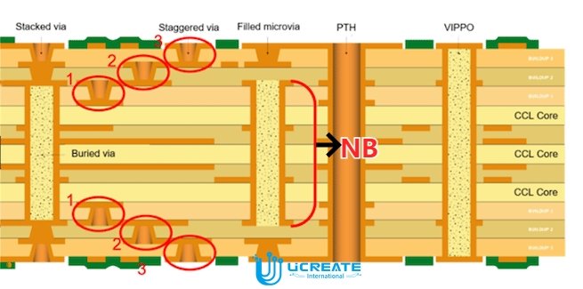
Here we present the existing support capabilities of NCAB: our offerings include type III structures featuring a central nucleus known as NB, accompanied by three sets of blind holes. We are also working on introducing NB +4 and +5 sequences in the near future. Additionally, our portfolio will soon include the ELIC structure, enabling interconnects across every layer, with a maximum capacity of 10 layers.)
Designing High-Density PCBs for manufacturability can be challenging due to the complexity of the manufacturing processes involved. Designers need to consider the capabilities and limitations of the chosen PCB manufacturer and ensure that the design can be reliably manufactured within their capabilities. Factors such as minimum drill sizes, minimum track widths, and layer registration need to be carefully considered to ensure successful fabrication and assembly. Collaboration and communication between designers and manufacturers are essential to address any design-for-manufacturability issues early in the design process.
Cost Considerations
HDI printed circuit boards, with their advanced interconnect technologies and complex manufacturing processes, can be more expensive than traditional printed circuit boards. The additional manufacturing steps, specialised materials and higher precision requirements contribute to higher production costs. Designers must balance the desired circuit density and performance with cost considerations. Iterative design optimisation and exploration of alternative manufacturing options can help mitigate cost challenges without compromising functionality and quality.
Conclusion
HDI PCB technology has become a game changer in the electronics industry, enabling compact, high performance electronic devices. By understanding the features, benefits and challenges associated with HDI PCBs, Ucreate International’s designers and engineers can realise their full potential to create innovative and cutting-edge electronic products. With continued development and research, high-density electronic board are expected to shape the future of electronics design and manufacturing.


