
 English
 中文
中文In the ever-evolving landscape of modern electronics, multilayer printed circuit boards have emerged as a critical component, playing a pivotal role in the advancement of various industries. As technology continues to advance at a rapid pace, the demand for smaller, more efficient and powerful electronic devices has skyrocketed. Multilayer circuit boards have become the backbone of these innovations, enabling the creation of complex circuits in compact form factors.
Definition and Composition of Multilayer PCBs
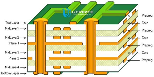
Multi layer printed circuit boards are advanced PCB that consist of multiple layers of conductive tracks and insulating material. Unlike single or double layer PCBs, which have only one or two layers of conductive material respectively, multilayer PCB board offer the ability to incorporate numerous layers into a single board.
The composition of multi-tiered PCBs typically includes alternating layers of conductive material, such as copper, and insulating material, known as the substrate or laminate. The conductive layers are typically copper foil, which is etched to form the desired circuit pattern. The insulating layers, also known as dielectric layers, are made of non-conductive materials, such as epoxy resin or polyimide, which provide electrical isolation between the conductive layers.
The number of layers in a multilayer board can vary depending on the complexity of the circuit and the design requirements. Typically, multi layer circuit board manufacturer can offer range from 4 to 20 or more layers, but there is no strict limit to the number of layers that can be incorporated. The layers are stacked and bonded using special adhesives to form a strong and compact structure.
To make connections between the different layers, multilayer printed circuit boards use vias. Vias are small plated holes that penetrate through the layers, allowing electrical connections to be made between traces on different layers. There are different types of vias used in multilayer PCBs, including through-hole vias, blind vias and buried vias, each of which serves a specific connectivity purpose.
Therefore, at Ucreate International, we believe that Multilayer circuit boards are an advanced printed circuit board consisting of multiple layers of conductive and insulating materials. They offer greater design flexibility, higher component density and improved signal integrity compared to single or dual layer PCBs. Through the use of vias and interconnect layers, complex circuit boards enable the creation of complex electronic systems within a compact form factor, making them an integral part of modern electronic devices.
Electronic devices reap the benefits of multilayer PCBs
1. Unparalleled Design Flexibility
Multilayer printed circuit boards offer unparalleled design flexibility, allowing Ucreate International’s engineers and designers to optimise the layout and functionality of electronic devices. With multiple layers, each serving a specific purpose, designers can assign different functional, signal and power layers to specific layers. This flexibility enables the creation of complex circuits while minimising space requirements. It also helps to integrate various components such as microcontrollers, memory modules and communication interfaces into a compact form factor.
2.Elevating Signal Integrity to New Heights
Signal integrity is crucial in modern electronic devices, especially those involving high-speed data transmission, such as smartphones, networking equipment, and high-performance computing systems. Multilayer PCBs excel in maintaining signal integrity by providing dedicated ground and power planes, which minimize electromagnetic interference (EMI) and crosstalk. The separation of sensitive signals from noisy signals on different layers reduces the likelihood of signal degradation, ensuring reliable and high-speed data communication.
3.Empowering Power Distribution Systems
Efficient power distribution is vital for the proper functioning of electronic devices, particularly those with high power requirements, such as servers, power supplies, and electric vehicles. Layered PCBs offer power planes that can handle high currents while minimizing impedance. This allows for stable power delivery to various components, reducing voltage drops and ensuring consistent performance. Additionally, the use of multiple power planes helps isolate sensitive analog and digital signals from power noise, further enhancing system reliability.
4. Redefining Size and Weight Reduction Strategies
Multi-level circuit boards play a significant role in the ongoing miniaturization trend of electronic devices. By incorporating multiple layers of circuitry into a single board, these PCBs enable the creation of smaller and more compact devices without sacrificing functionality. The ability to stack and interconnect layers allows for efficient space utilization, leading to reductions in the overall size and weight of the electronic device. This advantage is particularly valuable in portable devices, wearables, and aerospace applications with strict size and weight constraints.
5. Pioneering Component Density Evolution
Multi-layer circuit boards enable the integration of a higher number of components within a limited space, thereby increasing component density. With the ability to stack multiple layers and utilize vias for interconnections, designers can maximize the utilization of the available surface area. This advancement in component density allows for more functionality in compact devices, enables the implementation of advanced features, and contributes to overall system performance improvements.
6. Tackling EMI/EMC Challenges with Multilayer PCBs
Electromagnetic interference (EMI) and electromagnetic compatibility (EMC) are significant concerns in electronic design. Multi-layer circuit boards employ various design techniques to address these challenges. By properly separating sensitive signals from noise sources on different layers, utilizing shielding techniques, and implementing proper ground and power plane structures, complex circuit boards can effectively mitigate EMI/EMC issues. This ensures that electronic devices comply with regulatory standards and operate in environments with minimal interference, improving overall system reliability.
Mastering the Art of Designing with Multilayer PCBs
1. Crafting Optimal Layer Stackups and Signal Layer Placement
Designing with multi-stratum circuit boards requires careful consideration of layer stackups and signal layer placement. The layer stackup defines the arrangement of conductive and insulating layers in the PCB. It is essential to optimize the layer stackup to meet the specific design requirements, including signal integrity, power delivery, and thermal management.
When designing the layer stack, the Ucreate International design team considers several factors, including impedance control, signal layer separation, power and ground plane distribution, and high-speed signal routing. Strategic placement of signal layers near power and ground planes minimizes noise coupling and maintains signal integrity. Arranging power and ground planes symmetrically and balancing them ensures a robust power distribution system, reducing the risk of ground bounce and power plane noise.
2. Paving the Way for Robust Power and Ground Plane Implementation
Multi-sheet circuit boards offer excellent opportunities to implement strong power and ground planes. The power plane is a dedicated layer that distributes power to various components, while the ground plane provides a low-impedance return path for signals and acts as a shield against electromagnetic interference (EMI). It is imperative for Ucreate International engineering to ensure that the power and ground planes have sufficient copper area to minimize voltage drops and maintain signal integrity.
Proper implementation of power and ground planes requires careful consideration of layer layout, via layout, and plane stitching techniques. By strategically placing vias to connect power and ground planes, we can reduce loop area and inductance, thereby improving power integrity and reducing EMI. Additionally, using stitched vias to create a grid pattern of interconnects can enhance power and ground plane continuity, further improving performance and reducing noise.
3. Ensuring Signal Integrity and Impedance Control Precision
Signal integrity is of utmost importance in multilayer PCB designs, especially for high-speed digital signals. Our designers pay meticulous attention to impedance control and routing techniques to ensure optimal signal integrity. Impedance mismatch can lead to signal reflections, signal attenuation, and electromagnetic interference, which can be detrimental to the performance of the PCB.
To achieve precise impedance control, our designers consider various factors such as trace width, spacing, dielectric thickness, and the dielectric constant of the materials used. To achieve consistent signal propagation and reduce the risk of reflections and crosstalk, it is essential to use controlled impedance routing techniques, such as differential pairs and controlled impedance traces. By implementing these techniques, designers can ensure reliable and high-performance circuit board designs.
Additionally, careful routing techniques, such as minimizing trace lengths, avoiding sharp bends, and maintaining proper ground return paths, are critical to maintaining signal integrity.
4. Effective Thermal Management Strategies
Multi-level circuit boards often face thermal challenges due to the compact size and increased component density. Effective thermal management strategies are crucial to prevent component overheating, ensure long-term reliability, and maintain optimal performance.
Thermal vias play a vital role in dissipating heat from high-power components or areas with high heat dissipation. By strategically placing thermal vias in the vicinity of heat-generating components and connecting them to dedicated thermal planes or heat sinks, designers can efficiently transfer heat away from critical areas.
Additionally, designers can implement thermal relief patterns for surface mount components to enhance heat dissipation. Careful placement of components and heat sinks, as well as utilizing advanced thermal simulation tools, can help optimize the thermal performance of the multilayer PCB.
5. Guarding Against EMI/EMC Interference with Proactive Design Guidelines
EMI and EMC are ongoing challenges in electronic design. Designers must proactively incorporate EMI/EMC guidelines and techniques to minimize interference and ensure compliance with regulatory standards.
Some key design guidelines include proper grounding techniques, effective shielding, and the use of EMI filters and decoupling capacitors. Ground planes play a crucial role in providing a low impedance return path and reducing EMI. By ensuring proper ground connections, minimizing ground loops, and employing shielding techniques such as copper pours and shielding cans, designers can mitigate EMI issues.
Furthermore, integrating EMI filters and decoupling capacitors near sensitive components helps suppress unwanted noise and maintain signal integrity. Careful consideration of trace routing and signal isolation techniques also aids in reducing EMI/EMC interference.
Conclusion
Multiple-layer PCBs play a pivotal role in enabling advanced electronic designs and improving overall system performance. Their advantages, including increased design density, enhanced signal integrity, efficient power distribution and grounding, and effective thermal management, make them indispensable in modern electronic equipment. By considering the design considerations discussed in this article, designers can harness the full potential of Layered PCBs and create innovative and reliable electronic systems.
Our factory has advanced rigid multilayer board technology capability, can produce up to 64 layers, Outer copper thickness can be made more than 15 oz, Hole position tolerance only ± 0.025mm, whether it is difficulty PCBs, multilayer flexible PCBs or HDI multilayer PCB as well as assembly, we can solve well, to provide you with the optimal solution. Before production, we will do free DFM testing to ensure that your design file produced. Please feel free to send us your gerber file if you have any needs.
Here’s our offical email: sales@ucpcba.com


