 English
 中文
In the printed circuit board (PCB) manufacturing industry, product quality assessment covers a wide array of electrical, mechanical, thermal and dimensional parameters. Among all these inspection items, bow and twist stand out as one of the most fundamental yet easily overlooked mechanical specifications. Many purchasers and electronic design engineers focus heavily on impedance control, copper thickness, hole size tolerance and soldermask quality at the early stage of project evaluation, while failing to attach sufficient importance to PCB flatness. It is not until the SMT assembly line encounters continuous production failures, such as component tombstoning, poor solder joint formation, picking and placement errors of surface-mount devices, or even functional failure of finished electronic modules, that the engineering team traces the root cause back to excessive bow and twist of bare PCBs. For high-density electronics, automotive control boards, industrial controller PCBs, power supply modules and communication hardware, stable and controlled bow and twist performance is no longer an optional premium feature. It has become a baseline requirement to guarantee smooth mass production and long-term service stability of end products.
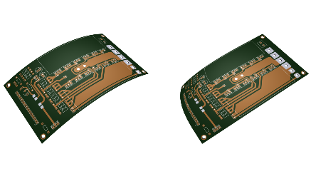
To fully understand bow and twist, we need to separate the two definitions clearly, as they describe two different types of board deformation, although they are always discussed together in PCB quality standards. Bow refers to the arc-shaped bending deformation of a PCB panel along its length or width direction. Imagine placing a rectangular PCB on a perfectly flat reference surface. When the board curves upward or downward like a shallow arch, this is bow. During measurement, the board’s four corners are kept in contact with the flat reference plane, and the maximum vertical gap between the board surface and the reference plane in the middle area is measured. The bow value is calculated as the ratio of this maximum gap to the corresponding board length, expressed as a percentage. Twist, by contrast, represents torsional distortion. It happens when one corner of the PCB lifts away from the flat reference surface while the other three corners stay attached to the plane, creating a twisted shape similar to a wrung towel. Twist reflects the uneven stress distribution across diagonal directions of the substrate.
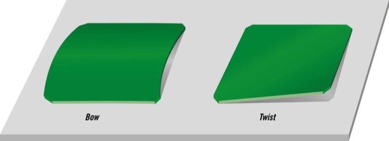
Industry standards such as IPC-A-600 and IPC-6012 have established universal testing and calculation rules for bow and twist. The standard formula is straightforward: Bow or Twist (%) = (Maximum measured deviation / Corresponding board dimension) × 100%. It is critical to note that bow and twist testing must be carried out under specified environmental conditions. Ambient temperature and humidity will affect the state of resin in the prepreg and substrate material, so testing is normally performed after the PCB completes all fabrication processes, including etching, soldermask coating, surface finish treatment, final baking and moisture stabilization. Only finished boards that have gone through full production and stress relief can provide valid bow and twist data. Unfinished semi-finished panels cannot represent the flatness performance of the deliverable product.
What is the practical purpose of testing and controlling bow and twist? The core value lies in supporting automated surface mount assembly and ensuring consistent solder quality. Modern electronics manufacturing relies on high-speed SMT placement machines. These machines use vacuum nozzles to grab tiny resistors, capacitors, IC chips, connectors and other SMD components and place them precisely onto solder pads. If the PCB is severely bowed or twisted, the pad positions will deviate from the programmed plane height. The placement nozzle may fail to press the component evenly onto the solder paste. Some pads will have insufficient solder paste contact, leading to open solder joints; some areas will suffer excess solder and bridging between adjacent pins. For fine-pitch ICs, QFN packages, BGA chips and 0201/01005 miniature passive components, the tolerance window for flatness is extremely narrow. Even a small amount of warpage can trigger massive assembly scrap.
Beyond SMT placement, reflow soldering is another key process affected by bow and twist. During reflow, the PCB passes through a furnace with staged temperature zones. The substrate, copper foil, prepreg and soldermask all expand and contract at different rates under heat. If the bare board already has large inherent bow and twist before reflow, thermal stress in the oven will further amplify deformation. BGA packages are especially sensitive: uneven warpage will separate the solder balls from the PCB pads in the central area of the component, creating hidden cold joints that cannot be detected by ordinary visual inspection. These hidden defects are extremely dangerous. The product may pass factory testing, but fail intermittently after being shipped to customers, under vibration or temperature cycling in the end application. Such field failures bring huge after-sales costs and damage brand credibility for electronic manufacturers.
Beyond SMT placement, reflow soldering is another key process affected by bow and twist. During reflow, the PCB passes through a furnace with staged temperature zones. The substrate, copper foil, prepreg and soldermask all expand and contract at different rates under heat. If the bare board already has large inherent bow and twist before reflow, thermal stress in the oven will further amplify deformation. BGA packages are especially sensitive: uneven warpage will separate the solder balls from the PCB pads in the central area of the component, creating hidden cold joints that cannot be detected by ordinary visual inspection. These hidden defects are extremely dangerous. The product may pass factory testing, but fail intermittently after being shipped to customers, under vibration or temperature cycling in the end application. Such field failures bring huge after-sales costs and damage brand credibility for electronic manufacturers.
Bow and twist control also matters for downstream processes after soldering. In some production lines, assembled PCBs need to be locked into plastic or metal housings. A warped board will force fit during assembly, introducing continuous mechanical stress on solder joints and components. When the end product works under alternating high and low temperatures, this residual stress accumulates over time and eventually causes solder cracking or component cracking. For products used in harsh environments, including automotive electronics, industrial automation equipment, outdoor communication terminals and new energy control boards, reliability requirements are far stricter than consumer electronics. Therefore, these customers always put forward clear bow and twist limits in their PCB specifications at the beginning of project cooperation.
Many PCB suppliers quote the general IPC default limit of 1.5% for bow and twist, which is the basic acceptance threshold for ordinary low-density, through-hole boards with few SMD parts. However, as electronic products keep shrinking in size and increasing in component density, 1.5% warpage is no longer acceptable for most mid-to-high-end applications. More and more customers are requesting 1.0% or even tighter limits. This is where our company builds our competitive advantage. Our stable production capability for PCB bow and twist is controlled within the range of 0.5% to 0.75%. This figure is not a laboratory test result from a small number of sample boards; it is the statistical performance of mass production batches, covering multi-layer boards, rigid FR-4 PCBs, boards with different copper weights, various surface finishes including HASL, ENIG, OSP, immersion silver and immersion tin, and different board sizes from small single pieces to large array panels.
Achieving stable bow and twist between 0.5% and 0.75% is never an easy target. PCB warpage originates from internal stress inside the board, and stress accumulates at every single manufacturing step. The source of stress includes the mismatch of thermal expansion coefficients between copper foil and dielectric material, asymmetric copper distribution on the top and bottom layers, uneven lamination pressure and temperature, improper curing profile of prepreg, uneven etching removal of copper, uneven soldermask coverage, uncontrolled cooling rate after high-temperature processes, and insufficient baking for moisture removal. Every subtle fluctuation in these parameters can push bow and twist out of the target range.
To lock bow and twist steadily at 0.5%–0.75%, we have built a full-process control system, starting from front-end engineering design review all the way to final outgoing inspection. At the engineering stage, our PCB layout engineers evaluate copper balance on top and bottom layers proactively. If one side has large solid copper planes while the opposite side has almost no copper, we will communicate with customers to add dummy copper patterns, adjust copper area distribution, and optimize stack-up structure. Reasonable stack-up design is the first and most effective way to reduce inherent warpage risk. During lamination, we strictly monitor the heating rate, peak temperature, dwell time and cooling curve of each press cycle. We avoid rapid heating and rapid cooling, which are major causes of residual stress. Different prepreg resin systems have unique curing characteristics, and we configure independent lamination recipes for each material type instead of using a universal program for all boards.
After lamination, drilling, desmear and copper plating also need careful handling. Uneven plating thickness will introduce asymmetric stress. Our factory maintains tight control over copper thickness uniformity across the whole panel. In the etching process, we optimize etching parameters to ensure consistent copper removal rate and minimize side effects from uneven etching. The soldermask process is another critical control point. Soldermask ink shrinks during UV curing and thermal curing. If one side of the board has a much thicker soldermask layer or a much larger soldermask coverage area, asymmetric shrinkage will bend the board. Our operators and QA team monitor soldermask coating thickness and curing parameters batch by batch.
Stress relief baking is a standardized mandatory step in our workflow before final inspection. After surface finish, boards go through controlled baking cycles to release residual moisture and internal stress slowly. Baking temperature, holding time and cooling method are defined according to board thickness, layer count and substrate material. Boards are stacked with separation sheets to prevent new deformation during cooling. For every production lot, we arrange random sampling for bow and twist measurement following IPC measurement methods. Our inspection team uses calibrated flat granite reference platforms and dial indicators to collect readings, records the data into our MES production system, and tracks the trend of bow and twist values continuously. If any sample approaches the upper limit of 0.75%, our process engineering team will launch an immediate review to identify process drift and adjust parameters before the whole batch is released.
Customers often ask what benefits they can obtain from our 0.5%–0.75% bow and twist capability compared with suppliers who can only meet the 1.5% standard or around 1.0%. The advantages are reflected directly on their SMT production lines. First, the placement yield rises significantly. With highly flat bare boards, pick-and-place machines run at full rated speed without frequent height alarm interruptions. Operators spend less time adjusting equipment and reworking defective units. Second, reflow soldering quality becomes more predictable. Lower initial warpage provides a safety margin for thermal deformation inside the reflow oven. The risk of BGA open joints and fine-pitch bridging drops visibly. Third, production scheduling becomes more stable. Customers do not need to reserve extra time and manpower to sort out warped boards when receiving incoming materials. Incoming quality inspection (IQC) failure rates related to board flatness are kept very low.
This capability makes our PCBs well suited for a broad spectrum of high-value applications. It serves automotive electronic control units, battery management system PCBs, industrial PLC and sensor boards, gigabit communication modules, medical device control circuits, high-speed storage hardware and precision test instruments. For these customers, stable flatness is equivalent to stable product reliability. Many of our long-term partners transferred their projects to us specifically because their previous PCB vendors could not consistently control bow and twist, resulting in recurring SMT losses. After switching, they saw a clear reduction in assembly rework rate and field complaint rate.
We also want to clarify an important point: 0.5%–0.75% is our typical stable range for standard rigid PCBs. For special board types such as ultra-thin PCBs below 0.8mm thickness, large-format panels, or boards with extremely unbalanced copper layouts, the achievable warpage value will be evaluated case by case during the quotation phase. Our engineering team will inform customers of the realistic expectation and propose design optimization suggestions in advance. We never overpromise performance that cannot be delivered in mass production. Transparent communication on bow and twist limits is part of our quality commitment.
In the electronics supply chain, competition is gradually shifting from simple compliance with basic standards to consistent control of subtle mechanical properties. Electrical performance can be verified by flying probe or electrical test, but flatness problems only fully reveal themselves once the board enters SMT assembly. A PCB with perfect electrical connectivity may still become a troublesome product if its bow and twist are out of control. This is why forward-looking electronic manufacturers regard bow and twist data as one of the key indicators to evaluate the manufacturing maturity and process control level of a PCB supplier.
Our company’s consistent mass-production performance of 0.5% to 0.75% bow and twist is not a marketing slogan. It is the outcome of years of accumulation in stack-up design, lamination technology, process parameter tuning, material management and quality inspection systems. Every process adjustment, every batch data record and every engineering discussion about copper balance contributes to keeping board warpage within this tight window. As electronic products keep moving toward higher density, lighter weight and more reliable operation under complex working conditions, the requirement for PCB flatness will only become stricter. We will keep optimizing our process framework, upgrading testing methods and accumulating experience on new substrate materials, to maintain this stable bow and twist level and support our customers in launching competitive, high-reliability electronic products with fewer manufacturing risks.
When you select a PCB supplier, do not only compare price, lead time and basic specifications. Take a closer look at their real, mass-produced bow and twist capability. The 0.5%–0.75% flatness performance we provide is the quiet, solid guarantee behind your smooth SMT production and long-term product reliability. It is the small but crucial detail that separates a qualified PCB from a truly dependable one.