PCB Design
PCB Layout Design Service
Ucreate International provides PCB Layout Design service, as the supplement to our PCB manufacturing and assembly service.
Our highly-skilled teams of designers are qualified engineers with over 15 years of experience, also are experts of design through PADs PowerPCB, Or CAD, and more.
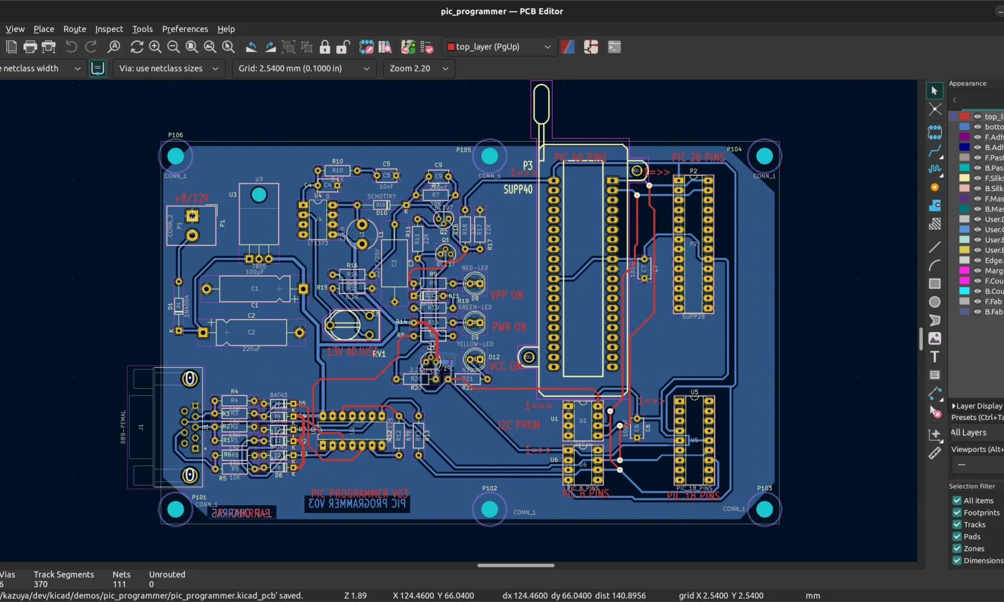

Ucreate International Have Designed Many Types Of Boards
- High speed digital circuits (video, audio, storage, etc.)
- Single/double sided,Flexible / flexi-rigid printed circuits (medical,home applications, etc.)
- High-power circuits (LEDs, power supplies, etc.)
- High-density interconnect circuits (smartphones, digital products, etc.)
- High-frequency circuits (communication devices, sensors, etc.)
Ucreate International offers reliable design
1.IPC class 2 and 3, JEDEC and MIL standards are available
2.Multilayer; through via hole, blind/buried via and laser via technologies
3.High density SMT designs (BGA, uBGA, PCI, PCIE, CPCI…)
4.HDI Designs with micro vias and advanced materials – Via-in-Pad, laser micro vias
5.High speed, multi layer digital PCB designs – Bus routing, differential pairs, matched lengths
6.DDR, DDR2, DDR3, DDR4, SAS and differential pair routing expertise
7.Ultra low EMI designs for MRI applications
8.Complete assembly drawings
9.In-Circuit Test data generation (ICT)
10.Drill, panel and cutout drawings design
What we can do for your PCB design?
Focusing on stability and long-term benefits in design, keeping up with the latest technologies and the updates of design platforms, which will avoid inefficient layouts and incompatibilities.
Taking into account the fluctuations in the component market and the ever-smaller size requirements, our design team works closely with the procurement teams in own PCB factory to provide the most forward-thinking solutions in the early stages of design, which will significantly reduce the time it takes to bring the product to market.
PCB layout design team have already got extensive board design experience, we will not make the revision again and again, everything is done in our mature DFM process and get through rigorously verified, which will reduce a lot of unnecessary revision expenses for the customers.
PCB component placement and routing are carried out by experienced and committed designers to ensure an optimal layout for your high speed logic and high frequency RF boards.


 English
 中文
中文


