
 English
 中文
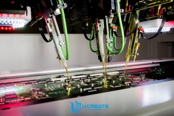
中文Flying probe test is a high-precision, non-contact electrical performance testing technology for PCBs (printed circuit boards). It uses a computer-controlled movable probe to contact test points on the circuit board, detecting continuity, short circuits, open circuits, and whether component parameters meet design requirements. Its core advantage lies in the fact that it eliminates the need for customized test fixtures, flexibly adapting to the testing needs of small batches and diverse product types, making it particularly suitable for sample verification and new product development stages.
Working Principle
The flying probe tester is equipped with 2-8 probes that can move precisely along the X, Y, and Z axes. Based on a preset program, it automatically positions itself to the PCB pads, vias, or component leads. By applying a small current or voltage signal, it measures parameters such as resistance, capacitance, and continuity to determine if the circuit has defects such as open circuits (broken lines), short circuits (abnormal continuity), or abnormal impedance. After comparing the test data with the design documents, the system automatically marks the fault location and generates a report.
Key Features
- High-Precision Positioning: The probe’s minimum positioning accuracy can reach 0.05mm, supporting high-density, fine-pitch circuit boards (such as mobile phone motherboards and chip carriers), and capable of detecting 01005 packaged components and linewidths below 0.1mm.
- High Flexibility: No test fixture fabrication is required; test programs can be quickly generated by importing Gerber files or CAD data, adapting to testing needs from single-sided boards to multilayer boards with 20 or more layers.
- Controllable Cost: Eliminates the cost of test fixture fabrication (typically thousands to tens of thousands of yuan), suitable for small-batch production (monthly capacity <1000 pieces) and rapid prototyping scenarios, reducing R&D costs by 30%-50%.
- Wide Testing Range: Can detect open circuits, short circuits, resistance/capacitance deviations, diode polarity, IC pin connectivity, etc. Some high-end models support impedance testing and high-frequency signal integrity analysis.
Test Flow
- Program Generation: Import PCB design files (e.g., Gerber, netlist), automatically extract test point coordinates and netlist information, and generate probe movement paths.
- Positioning and Testing: After the PCB is fixed by the conveyor mechanism, the probes contact the test points according to the program, sequentially completing continuity testing (open circuit/short circuit) and component parameter measurements (resistance, capacitance, etc.).
- Data Analysis: Real-time comparison of measured values with standard values, marking out-of-tolerance items; supports double-sided testing, using top and bottom probes to cover blind and buried vias on multilayer boards for testing.
- Report Output: Generates a visual fault distribution map, marking defect types (e.g., “R123 open circuit”, “Net5 short circuit”) and specific coordinates for easy rework.

Applicable Scenarios
- R&D Prototyping: Rapidly verify design rationality at the sample stage, shortening iteration cycles, especially suitable for rapidly iterating products such as consumer electronics and IoT.
- Small-Batch Production: Suitable for multi-variety, customized orders (e.g., medical equipment, military electronics), avoiding idle and wasteful test fixtures.
- Complex Board Testing: Suitable for high-density PCBs (BGA/CSP packages), flexible printed circuit boards (FPCs), and circuit boards made of special materials such as ceramic substrates.
Limitations:
- Relatively slow testing speed: Single-pin testing speed is approximately 10-40 points/second. For mass-production boards (e.g., daily capacity exceeding 1000 pieces), efficiency is lower than that of test fixture testing (ICT), requiring a balance between capacity and cost.
- Probe wear: Long-term use may cause tip wear to affect accuracy, requiring periodic calibration (recommended every 500 pieces tested).
- Limitations on some parameters: Cannot directly test dynamic circuit performance (e.g., chip function); requires use in conjunction with AOI (Optical Inspection) or X-ray.
Ucreate PCB factory can produce 200,000 SQM/month, which have advanced equipment and test technologies and automated equipment like automated immersion gold line, automated PTH line, automated plating line and automated CNC drilling machined, etc. At Ucreate, we provide comprehensive PCB and assembly testing services to ensure that your electronic products meet the highest quality standards. We provide microsectioning test, AOI test, ICT test, flying probe test, X-Ray inspection, functional test, RoHS test, etc.

Summary
Flying probe test, with its flexibility and high precision, has become an indispensable quality control component in PCB manufacturing, demonstrating significant advantages, especially in R&D and small-batch production. When choosing this method, a comprehensive evaluation based on production volume, board complexity, and cost budget is necessary—flying probe testing is preferred for the sample stage, while switching to test fixture testing is recommended for mass production to improve efficiency.


