
 English
 中文
中文In multilayer PCB manufacturing, vias are key structures that connect different circuit layers.With the development of electronic devices towards miniaturisation and high density, via plugging technology has emerged.This process through physical or chemical methods to fill or close the hole, in order to solve the traditional hole brought about by a variety of problems.
In modern PCB design, the diameter of the vias is getting smaller and smaller (commonly 0.1-0.3mm), and the thickness of the copper layer on the wall of the vias is usually in the range of 15-25 μm. These tiny structures in the untreated state are prone to become the weak links of the PCB, and the hole plugging process can significantly improve this situation.
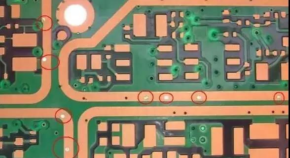
I. The main role of over-hole plugging
Preventing Solder Loss
During the soldering process, especially the surface mount (SMT) process, solder may flow from the pads into the vias, resulting in poor soldering.Plugging the holes effectively prevents solder loss and ensures solder quality.
Improve circuit board reliability
Avoid flux, cleaning agent and other liquid residue in the hole to prevent corrosion or short circuit.
Reduces the risk of hole wall cracking caused by thermal stress and enhances the mechanical strength of the PCB.
Improve Surface Flatness
Plugging holes makes the PCB surface flatter, especially in high-density interconnect (HDI) boards, which facilitates the placement and soldering of fine-pitch components.
Optimise electrical performance
In high-frequency circuits, unplugged vias can cause signal reflections or crosstalk, and plugging the vias reduces these interferences and improves signal integrity.
II. Common methods of plugging holes
Process Type | Cost Index | Minimum Hole Diameter | Flatness | Conductivity | Typical Applications |
Resin Plug Hole | 1.0x | 0.15mm | ★★★★ | Insulation | Consumer electronics, industrial control equipment |
Plating Hole Filling | 2.5x | 0.10mm | ★★★★★ | Conductive | Servers, 5G devices |
Conductive Adhesive Hole Filling | 1.8x | 0.12mm | ★★★★☆ | Conductive | Automotive electronics, military products |
Solder Resist Plug Hole | 0.6x | 0.20mm | ★★☆☆ | Insulation | Low-end consumer products |
III. Technical points for process selection
High frequency application scenarios
- Prefer plating to fill holes (more stable dielectric constant)
- Recommended with laser drilling (hole diameter ≤ 0.1mm)
- Copper thickness control at 18±2μm is optimal.
High reliability requirement
- Resin plugging + surface plating combination process is recommended
- Filling material should be UL approved
- Coefficient of thermal expansion should match the substrate (typically 6-8ppm/°C)
Cost sensitive products
- Selective plugging strategy available
- Plugging only below critical pads
- Optimised in conjunction with soldermask window design
summaries
Over-hole plugging has evolved from a mere process option to a necessary consideration in PCB design.With the advancement of 5G, AI, IoT and other technologies, hole plugging technology will continue to evolve.Engineers need to find the best balance between cost, performance, and reliability, and an in-depth understanding of the characteristics and applicable scenarios of various hole plugging processes is the basis for making the right choice.In the future, intelligent plugging solution selection and automated plugging quality inspection will become an important direction for the development of the industry.


