As circuit speeds increase, signals in the CHz range are common. Therefore, controlled trace impedance plays an important role in signal integrity and board performance.
What is PCB impedance control?
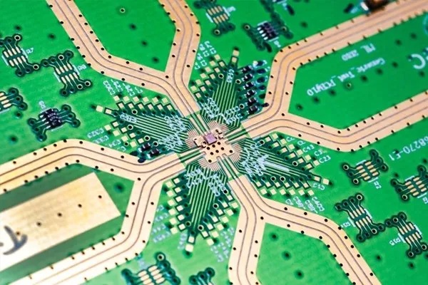
PCB impedance control involves controlling trace impedance, also known as controlled impedance. Controlled impedance is the characteristic impedance of a transmission line formed by a PCB trace and its associated reference plane. This impedance is relevant when high-frequency signals propagate along a PCB transmission line. Controlled impedance is crucial for addressing signal integrity issues, which focus on ensuring distortion-free signal transmission.
The impedance of a circuit is determined by the physical dimensions and dielectric material of the PCB. It is measured in ohms (Ω). PCB transmission line types that require controlled impedance include single-ended microstrip, single-ended stripline, microstrip differential pair, stripline differential pair, embedded microstrip, and coplanar (single-ended and differential).
Why is it necessary to control PCB impedance?
Typically, you need to control PCB impedance for high-speed digital applications such as RF communications, telecommunications, computing using signal frequencies above 100MHz, high-speed signal processing, and high-quality analog video (e.g., DDR, HDMI, Gigabit Ethernet), etc.
At high frequencies, signal traces on a PCB behave like transmission lines, with impedance present at every point along the trace. If this impedance varies from one point to the next, a signal reflection will occur, the amplitude of which will depend on the difference between the two impedances. The greater the difference, the greater the reflection. This reflection will propagate in the opposite direction of the signal, meaning that the reflected signal will be superimposed on the primary signal, distorting the original signal.
A signal originally intended for transmission undergoes changes once it reaches the receiving end. This distortion can be so significant that the signal may no longer perform its intended function. Therefore, to achieve distortion-free signal transmission, PCB signal traces must have uniform, controlled impedance to minimize signal distortion caused by reflections.
Uniform transmission lines on a PCB have a defined trace width and height and are located at a consistent distance from the return path conductor, usually a plane at a certain distance from the signal trace.
Factors Affecting PCB Controlled Impedance
Factors that affect PCB impedance tolerance include the material’s resin content percentage, the resin’s Dk value, and the type of glass cloth used, as well as other physical PCB tolerances such as trace height and width at the top and bottom of the trace.
When you need to manufacture PCBs with the correct pattern sizes and positions within a certain tolerance range, you must ensure that the manufacturer provides the correct size, position, and tolerance of the etched features. Otherwise, each of your PCBs will be different, making it very difficult to debug performance-related issues.
Future Horizons
As we look ahead, three trends will shape impedance control PCBs:
Co-packaged Optics: Silicon photonics will place 51 Tb/s switch ASICs millimeters from optical engines. PCB traces will shrink to millimeter lengths but must still maintain 50 Ω single-ended control for bias and modulation lines.
3-D Integration: Embedded trace substrates (ETS) and sequential build-up (SBU) technologies will route signals through 20+ layers with aspect ratios exceeding 20:1, demanding sub-micron impedance accuracy.
AI-Driven Manufacturing: Machine-learning models trained on terabytes of TDR data will predict impedance excursions before panels leave the press, enabling real-time correction and zero-defect shipments.

 English
 中文
中文


