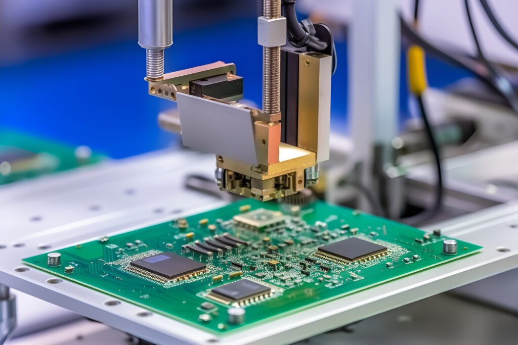
A PCB prototype, short for Printed Circuit Board prototype, is an early version or sample of a printed circuit board that is created for testing and evaluation purposes before mass production. It serves as a crucial step in the product development cycle, allowing designers and engineers to validate the design, functionality, and performance of the circuit.
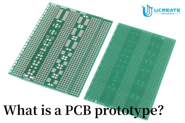
A PCB is a board made of insulating material, such as fiberglass, with conductive pathways etched or printed onto its surface. These pathways, known as traces, connect various electronic components, such as resistors, capacitors, and integrated circuits, forming a functional electronic circuit.
The Main Benefits of Developing PCB Prototypes
PCB prototyping service offers several key benefits that can significantly enhance the design and development process. These benefits help to ensure a successful, efficient product launch. Let us at Ucreate International’s technical department explore them in detail:
1. Iterative Design
Quick turn PCB enable iterative design cycles, allowing for continuous improvement and optimization of the circuit design. Designers can quickly test and evaluate different iterations, make modifications, and fine-tune the circuit layout. This iterative approach helps refine the design by addressing potential issues and optimizing the performance, leading to a higher-quality final product.
2. Functionality Testing
Fast PCB prototyping play a crucial role in validating the functionality and performance of the circuit. Through testing, designers can assess whether the circuit operates as intended, meets the desired specifications, and performs reliably under various conditions. Functionality testing helps identify any design flaws, compatibility issues, or performance limitations, allowing for necessary adjustments and improvements.
3. Identifying Design Flaws
PCB prototypes are instrumental in identifying and rectifying design flaws early in the development process. By physically implementing the circuit design and testing it in a real-world scenario, designers can uncover potential issues that may not be apparent in simulations or on paper. Detecting and addressing these flaws at the prototype stage helps avoid costly rework or product recalls during mass production, saving both time and resources.
4. Cost and Time Savings
PCB prototypes can lead to significant cost and time savings in the long run. By catching and resolving design flaws early on, the need for expensive modifications or redesigns during mass production can be minimized. Additionally, identifying and rectifying issues at the prototype stage reduces the risk of delays and ensures a smoother transition to large-scale manufacturing. This streamlined process ultimately shortens the time-to-market, allowing companies to seize market opportunities more efficiently.
The benefits of developing prototype pcb and assembly are many and powerful. It enables iterative design cycles, verifies functionality, identifies design flaws and helps to save costs and time. By leveraging these benefits, companies can improve the overall quality, reliability and market competitiveness of their products. PCB prototypes are an essential tool in the product development process, helping to ensure a successful and efficient product launch.
Commonly Used Methods for PCB Prototyping
1. Breadboarding
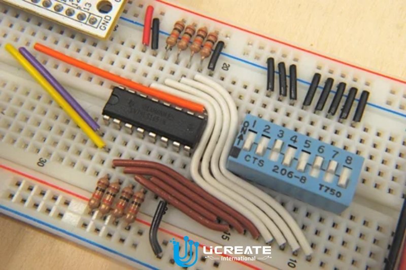
Breadboarding is a popular method for quick and temporary circuit testing. It involves using a breadboard, which is a reusable platform with a grid of interconnected holes. Components are inserted into the breadboard, and their leads are connected through the holes using jumper wires. Breadboarding allows designers to quickly assemble and test circuits without the need for soldering. While breadboarding is convenient for initial testing and proof of concept, it may not be suitable for complex or high-frequency circuits.
2. Printed Circuit Prototyping
Printed circuit prototyping involves the in-house manufacture of PCB prototypes using various techniques such as etching and milling. In etching, a layer of resist is applied to a copper-clad board to expose the desired circuit pattern, and then an etchant solution is used to etch away the unwanted copper. This leaves the desired copper traces. Milling, on the other hand, uses a computer-controlled milling machine to remove unwanted copper from the board and form the desired circuit pattern. Circuit board prototyping offers greater accuracy and reliability than breadboarding, but requires specialised equipment in our production department and expertise from our engineering department.
3. PCB Manufacturing Services
Designers provide PCB layout files and manufacturing services take care of fabrication, component placement, soldering and quality control. Ucreate International uses advanced manufacturing processes such as Surface Mount Technology (SMT) to produce high quality prototypes with faster turnaround times. This method is suitable for complex designs, high frequency circuits or when large numbers of prototypes are required.

The choice of PCB prototyping method depends on factors such as the complexity of the design, available resources, time constraints, and budget. Breadboarding is ideal for initial testing and concept validation, while printed circuit prototyping is suitable for in-house production with moderate complexity. PCB manufacturing services offer higher precision and scalability for more advanced designs or larger prototype quantities.
By leveraging these different methods, designers and engineers can select the most appropriate approach for their specific prototyping needs, balancing cost, time, and quality considerations.
Conclusion
PCB prototyping is a critical step in the product development process, offering numerous benefits and playing a vital role in ensuring the success of the final product. By summarising the importance of PCB prototyping and highlighting the importance of choosing the right prototyping method, we can understand its overall impact on the product development process. One of the key benefits of PCB prototype manufacturing is its ability to facilitate functional testing.
By physically implementing a circuit design and subjecting it to real-world conditions, designers can evaluate its performance, functionality and compatibility. This testing phase helps to ensure that the final product meets the required specifications and performs reliably in a variety of scenarios. PCB prototyping is an integral part of the product development process, providing benefits that contribute to the overall success of the final product. By emphasising the importance of choosing the right prototyping method, designers can take advantage of PCB prototyping to refine their designs, verify functionality and simplify the path to successful mass production.
Related Post
- The Complete Guide to Successful BGA Package Design: From Concept to Production
- PCB Layout Development for In-Circuit Testing Systems: Where Signal Integrity Meets Test Coverage
- Chinese New Year Holiday Notice
- What is PCB DFM?
- Technical Specifications for PCB Through-Hole Component Hole Diameter Design

 English
 中文
中文


