
 English
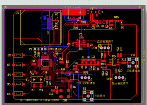
 中文
中文When designing a printed circuit board (PCB), layout is a key component in determining circuit performance, reliability and manufacturing costs. Proper layout not only ensures signal integrity, but also improves thermal efficiency and manufacturability. This article describes the basic layout rules to follow in PCB design:
1. Spacing rules
- Minimum spacing: Spacing between wires, between wires and pads, and between wires and vias should be maintained at a certain distance, usually recommended to be ≥ 0.2 mm, and can be increased to 0.3 mm or higher for high-density designs to avoid short circuits and crosstalk.
- High-voltage circuits: For high-voltage circuits, higher safety spacing is required, typically ≥0.5 mm, depending on voltage level and insulation requirements.
- Pitch and dielectric material: Pitch design needs to take into account the dielectric constant and insulation properties of the PCB substrate to ensure electrical safety margins.
2. Direction of routing
- Preferred direction: Try to use horizontal, vertical or 45° angle layout, avoid using 90 ° right angle or sharp angle, in order to reduce signal reflection and electromagnetic interference (EMI).
- Adjacent Layer Cabling: In multilayer board design, the alignment of adjacent layers should be perpendicular to each other (e.g. one layer of horizontal cabling, another layer of vertical cabling) to reduce inter-layer coupling and crosstalk.
- High-speed signal layout: For high-frequency signals (e.g. HDMI, USB), give priority to 45° angle or curve wiring to reduce impedance mutation.
3. Wire width and thickness
- Selection of line width: Select the appropriate line width according to the amount of current. Typically, a line width of 1 mm on a 1 oz copper foil can carry about 1 A. For high current paths, a line width of ≥1.5 mm is recommended.For high current paths, line widths ≥ 1.5 mm are recommended.
- Minimum Line Width: The minimum line width supported by the standard process is 4 mil (0.1 mm), 2 mil (0.05 mm) can be used for high density designs, but manufacturer capabilities need to be confirmed.
- Wire Thickness and Heat Dissipation: Thicker copper foils (e.g. 2 oz or 3 oz ) increase current carrying capacity and heat dissipation efficiency, but can be more difficult to process.
4. Design of perforations
- Number of vias: Minimise the use of vias, which introduce additional inductance and resistance, affecting signal integrity.
- Vias Size: Commonly used vias are 0.8 mm in diameter and pads are 1.6 mm in diameter to ensure mechanical strength and solder reliability.
- Blind and Buried Holes: For High Density Interconnect (HDI) boards, blind or buried vias can be used to reduce wiring footprint.
5. Return pathways
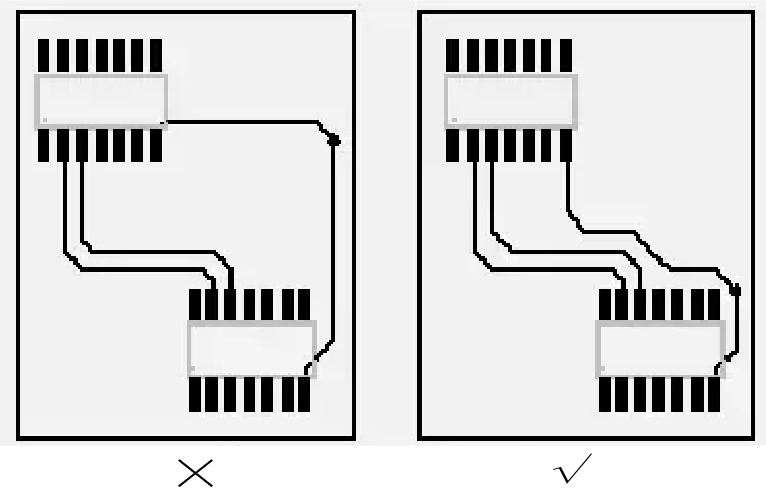
- Full Return Path: Provide a full return path for each signal line (especially for high frequency signals), usually through the ground plane (GND) to avoid interrupted or excessively long return paths.
- Multilayer board design: In multilayer PCBs, ensure that each signal layer has an adjacent ground plane or power plane to provide a low impedance return path.
- Reduce Loop Area: The return path for high-speed signals should be as close as possible to the signal lines to reduce the ground loop area, thereby reducing electromagnetic emissions (EMI) and ground bounce noise.(As shown below)
6. Differential pair layout
- Line Length Matching: Differential pairs should be matched within ±5 mil (0.127 mm) to avoid timing deviations and signal distortion.
- Spacing control: Differential pairs are typically spaced three or more times the line width to minimise crosstalk while maintaining differential impedance matching.
- Shielding design: Add a protective ground wire or design a shield around the differential pair to prevent external interference.
7. Power and signal cables
- Power cable width: The power cable should be as wide as possible, and a width of 1.5 mm or more is usually recommended to reduce resistance and heat generation.
- Signal line isolation: The signal line should avoid parallel wiring with the power line over long distances, and if necessary, it can be isolated by the ground line to reduce the interference of power supply noise on the signal.
- High-frequency power supply design: For high-frequency switching power supply, use multi-layer board design, and arrange the power plane adjacent to the ground plane to optimise electromagnetic compatibility (EMC).
8. Thermal management
- Thermal vias: For high power components (e.g. MOSFET, IGBT), use an array of thermal vias (e.g. 8×8 matrix ) with 0.3 mm or larger apertures to improve thermal efficiency.
- Thermal isolation: Keep high power components at least 3 mm away from sensitive components (e.g.oscillators, sensors) to avoid thermal conduction affecting performance.
- Large-area copper foil: Utilise a large-area copper foil as a heat sink area, directly connected to the heat sink plane (GND or heat sink).
9. Cabling cascade design
- Single-layer board: Suitable for simple circuits, giving priority to power and ground lines, and avoiding crossover of signal lines as much as possible.
- Double-layer board: One layer is used for signal lines, and the other layer is fully laid ground plane (GND) or power plane to enhance signal integrity.
- Multi-layer boards: Multi-layer design is recommended for complex circuits, e.g.
- 4-layer boards: Signal Layer – Ground Plane – Power Plane – Signal Layer
- 6-layer boards: Signal Layer – Ground Plane – Power Plane – Signal Layer – Ground Plane – Signal Layer
- 8-layer and above: Adding more pairs of signal layers and ground planes to support high-speed and high-density designs.
At the heart of PCB routing rules is balancing electrical performance, signal integrity, thermal efficiency and manufacturing feasibility.By following the basic rules of spacing, orientation, return paths, and differential pair routing, PCB reliability and performance can be significantly improved.At the same time, special design optimisation is required for high-speed signals, RF signals and thermal management needs.Whether you are a beginner or an experienced engineer, the reasonable application of these rules can help you design an efficient and reliable PCB.
If you need professional PCB layout design, please feel free to contact us, you can ask us for any requirements Ucraete team will offer you best solution.Our offical email: sales@ucpcba.com


