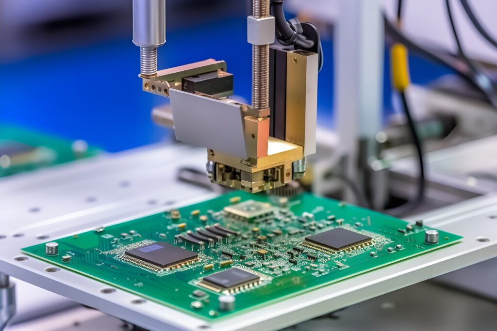
During PCBA processing, board warpage is a common problem that affects product reliability.This structural change may lead to soldering defects, electrical connection failure and even physical damage to the device.In this paper, we will systematically analyse the five core factors that lead to PCB warpage and provide technical references.
1. Improper selection of raw materials
- Coefficient of thermal expansion (CTE) of the base material mismatch: ordinary FR-4 sheet CTE is about 14-17ppm / ℃, while the copper foil CTE is only 17ppm / ℃.If you choose a low Tg value (glass transition temperature) materials (such as Tg ≤ 130 ℃), high-temperature reflow soldering is prone to internal stress.
- Uneven distribution of copper foil thickness: the difference in heat dissipation between the large copper area and the fine line area will form a local stress concentration.
2. Unreasonable design
- Layout asymmetry: component distribution bias, over-hole layout imbalance leads to asymmetric contraction force during cooling.
- Board design defects: V-cut dividing line is too close or improperly designed stamp holes will destroy the overall rigidity.
Design suggestion: Key devices should be arranged symmetrically, and the density of perforations should be evenly distributed to avoid local heat conduction imbalance.
3. Manufacturing process problems
- Lamination process control: Insufficient adhesive content or uneven lamination pressure of semi-cured sheets (PP sheets) will lead to differences in interlayer bonding.
- Drilling and plating process: Inadequate plating of blind/embedded holes will form heat transfer bottlenecks and local overheating will lead to deformation.
- Forming process impact: V-cut depth exceeds the standard or improper milling cutter speed/feed parameters directly lead to mechanical stress residue.
4. Temperature differences
- Reflow Temperature Profile: Temperature rise rate in the preheating zone >2℃/s will lead to rapid expansion of the material, and the risk of deformation will surge when the peak temperature exceeds the Tg value by 10-20℃.
- Ambient temperature fluctuations: Clean room temperature difference > ± 5 ℃ (especially in winter / summer) will exacerbate the material stress release.
5. Multilayer board connection point limitation
- Distribution of blind holes in the inner layer: Blind holes too close to the edge of the plate can limit the space for Z-axis expansion, leading to “bowing” warpage.
- Differences in plating filler: Inconsistent filler heights between layers can lead to differences in shrinkage during cooling.
Comprehensive solution proposal
Material Selection: Highly reliable plates with Tg≥150℃ and CTE matching (e.g. Megtron 6) are preferred.
Design Optimisation: Adoption of “Symmetric Design + Thermal Expansion Simulation” dual verification.
Process control: SPC monitoring of lamination parameters and segmented temperature control strategy for reflow soldering.
Means of inspection: Introduction of online AOI warpage inspection (standard: IPC-6012 Class 2 <0.75%).
PCB warpage risk can be effectively reduced through systematic material selection, design optimisation and process control.It is recommended to establish a full-flow quality control system from DFM (design for manufacturability) to process validation, which is especially important for high-reliability applications such as high-density interconnect (HDI) boards and automotive electronics.

 English
 中文
中文


