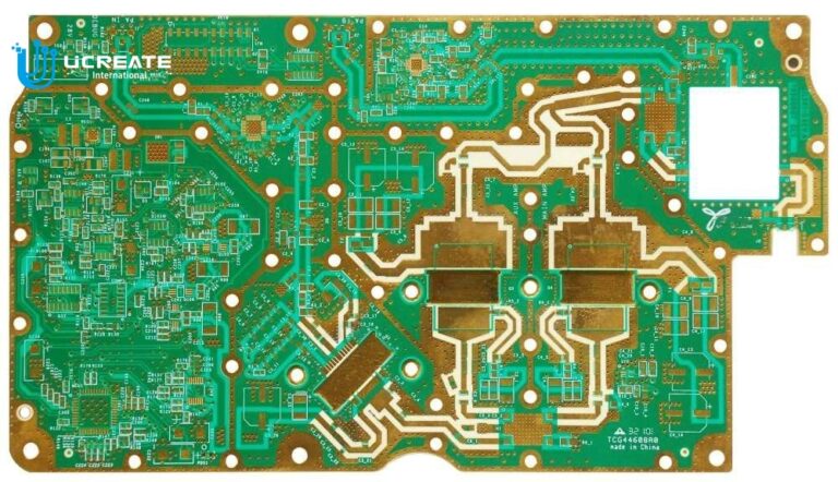
Radio Frequency (RF) PCB are very high speed circuits that operate at frequencies of 100mhz and above, typically between 500mhz and 2ghz.RF PCBs are the backbone of high tech devices such as wireless networks, smart phones, and smart TVs. In addition, RF printed circuit boards are used in automotive, medical device, military and aerospace applications for proficient measurement, detection and monitoring functions.
RF circuits are significantly different from any typical analog and digital circuits. RF signals consist of high-frequency analog signals that can be at any voltage or current level within set limits, at any given point in time. The design of such RF PCBs is quite complex and strict guidelines must be followed to mitigate interference problems caused by high frequency signals.
In the RF PCB design process, it is important to choose an experienced RF PCB supplier.
Ucreate has over 19 years of PCB manufacturing experience. The substrate material you choose determines price, thickness, circuit layout, mounting possibilities, etc. and covers a large part of the overall product functionality.

How to Choose the Right Laminate Substrate for HF RF PCBs
1. Matching the dielectric constant (Dk) of the resin and the substrate braiding material is highly recommended. Uneven Dks in the substrate can cause problems in high frequency operation. In PCB design, the designer must ensure that the Dk’s of all substrate layers match.
2. The degree to which a substrate expands in response to temperature changes during PCB fabrication or operation is known as the coefficient of thermal expansion. Different layers of a laminated substrate may expand at different rates, leading to functional failures and reliability issues. In RF PCB design, matching the CTEs of all substrate layers is a must.
3. Selecting a laminate substrate with a tight mesh with braided properties is recommended as it may directly affect Dk.
4. The loss tangent of the material is the energy lost in the dielectric region during signal transmission. In RF PCB design, choosing the correct loss tangent material is critical to signal integrity. PolytetrafluoroethylenePolytetrafluoroethylene (PTFE) material is one such material recommended for RF PCB design.
5. The chosen substrate should absorb a minimum amount of moisture from the environment to avoid any performance degradation at high frequencies.
6. Current signals tend to concentrate in a small area near the trace surface at high frequencies. This is known as the skin effect. The use of smooth copper foils in high frequency operation reduces this resistive loss.
General Design and Layout Guidelines: Building a High Quality RF PCB
1. The main concern is the sensitivity of high-frequency signals to noise interference, such as ringing, reflections or crosstalk. This requires careful impedance matching when routing RF signals. A common impedance value of 50ω is widely used by designers to simplify impedance matching of RF signals.
2. The inductance factor also has a significant impact on RF design and must be kept as low as possible. Make sure that RF components have adequate ground connections and that there are no discontinuities in the loop.
3. Traces connecting RF components must be short and sufficiently spaced to avoid any crosstalk problems.
4. Isolation of the RF traces is necessary to avoid any overheating problems as these tracks operate at a very high frequency. This can be achieved by stitching through holes around the RF traces.
5. A well balanced stack with uniform copper layer thickness improves the signal integrity of the RF PCB.
6. To avoid coupling effects, high speed signal traces should be routed on a different layer than the RF signal.
7. Power supply lines should be routed on dedicated power racks, inserting the necessary decoupling and bypass capacitors.
8. The addition of vias on RF traces and near-RF components reduces parasitic inductive effects and also reduces coupling between RF signals and other signal traces on the PCB.
Design Guidelines for RF PCB Assembly
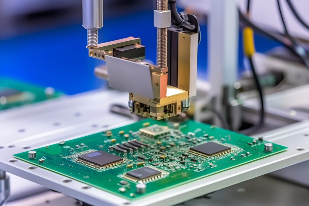
RF PCBs can be manufactured at high output by following some basic design guidelines required for RF PCB assembly. These rules are an extension of the standard DFM rules and will help to manufacture high output, high speed RF PCBs.
1. RF designs require higher power support. Therefore, thermal pads should be constructed for basic power needs and can still be fabricated for the amount of heat release required.
2. Placement of patch components must be considered well in advance of the component placement stage. In RF design, many metals are used for power networking and shielding purposes. These metal spaces should not be used by the designer to place any SMT components.
3. The complex signal routing requirements of RF PCBs can lead to strict component layout strategies. However, the designer must consider necessary rework, debugging requirements during mass production, and must provide adequate space for component access.
Guidelines for Safe Handling of RF PCBs
The boom in wireless technology has ensured the need for high frequency RF PCBs in consumer products alongside traditional military or aerospace applications. The increasing number of RF-based products has resulted in a crowded RF spectrum and unwanted interference. Therefore, it is necessary to handle these RF PCB applications with care.
Shielding RF circuit boards and their sensitive components can greatly reduce the threat of EMI interference. But this shielding may also interfere with signal transmission. To deal with EMI problems, proper PCB grounding is very important. Lengthy high-speed traces can act as transmitters and receivers of EMI. Therefore, adhering to the shortest possible trace length is important for any RF PCB design.
RF PCB design and fabrication requires good domain knowledge and detailed PCB fabrication experience. This comprehensive guide provides a combination of design, assembly and safety factors to be considered while designing an RF PCB. don’t forget to involve your PCB assembly supplier from the design stage to bring high performance RF PCBs to market.

 English
 中文
中文


