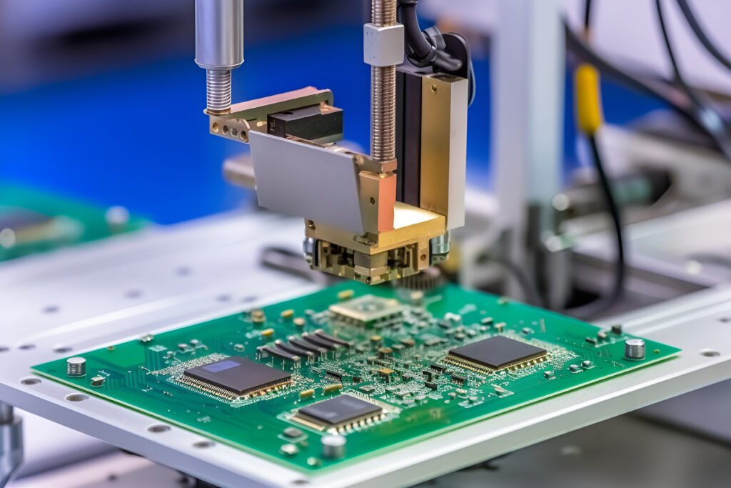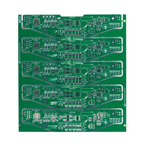
Ucreate 6 Layers HASL PCB Circuit Board
| Layers: | 6 L |
| Material: | Fr4 |
| PCB Thickness: | 1.2mm |
| Cu Thickness: | 1.0 OZ |
| Min. Line W/S: | 0.075/0.075mm |
| Surface Finish: | HASL |
| Application: | Consumer Electronics |
What is HASL?
HASL (Hot Air Solder Leveling) is one of the most commonly used surface finishing methods in the PCB industry. It is available in two types: leaded and lead-free. In addition, HASL is also one of the lowest-cost PCB surface finishing methods. This article will provide a detailed analysis of the advantages and disadvantages of hot air solder leveling.
During the manufacturing process, in order to obtain a HASL surface finish, the circuit board is immersed in molten solder (a tin/lead mixture). Doing so causes the solder to cover all exposed copper surfaces on the board. The board is then removed from the molten solder and high-pressure hot air is blown across the surface through an air knife to level the solder deposits and remove excess solder from the surface of the board.
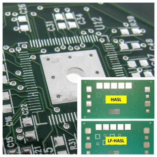
HASL finishing is now widely used in SMT processes. There are three main points:
• PCB should be immersed in molten solder;
• Before the solder solidifies, the wind knife blows the liquid solder away;
• The air knife can minimize the meniscus of the copper surface solder and prevent solder bridging.
Advantages:
• Cheap/low cost
• Longer storage time
• After the PCB is finished, the pad is completely covered with tin before soldering
• Lead-free (RoHS compliant) models are widely available
• Mature surface treatment options
• Visual inspection and electrical measurement are possible
Disadvantages:
• Poor flatness due to the natural meniscus of molten solder
• Not applicable to capacitive touch switches
• Cannot be used in high density interconnect (HDI) structures
• Not suitable for fine spacing
If you have any requirements for PCB/ PCBA/Components, please contact us and we will reply to you as soon as possible!


 English
 中文
中文


