
Free cookie consent management tool by TermsFeed

SMD vs. SMT: Unraveling the Connection and Differences in PCB Assembly

In the dynamic world of printed circuit board (PCB) and PCB assembly, two acronyms—SMD and SMT—are frequently mentioned, often leading to confusion among those new to the industry, and even some professionals who may mix up their roles and significance. For businesses and individuals relying on high-quality PCB solutions, understanding the relationship and distinctions between Surface Mount Devices (SMD) and Surface Mount Technology (SMT) is not just a matter of technical knowledge, but a key factor in ensuring the reliability, efficiency, and cost-effectiveness of electronic products. As a leading provider of PCB manufacturing and PCB assembly services, we aim to demystify these two core concepts, exploring how they work together to power modern electronics and what sets them apart. This article will break down their definitions, core connections, key differences, and practical applications in PCB assembly, helping you make informed decisions for your electronic projects.
What Are SMD and SMT?
Before diving into their connection and differences, it is essential to establish a clear understanding of what SMD and SMT actually are. Both are foundational to modern PCB assembly, but they represent entirely different aspects of the manufacturing process—one is a type of component, and the other is a method of assembly.

Surface Mount Devices (SMD): The “Building Blocks” of PCBs
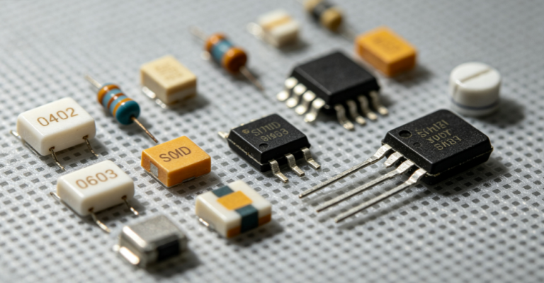
SMD, short for Surface Mount Device, refers to a category of electronic components specifically designed to be mounted directly onto the surface of a printed circuit board, rather than being inserted through holes (as with traditional through-hole components). These components are the physical “building blocks” that make up the circuitry of electronic devices, ranging from small consumer gadgets like smartphones and smartwatches to industrial equipment, automotive electronics, and medical devices.
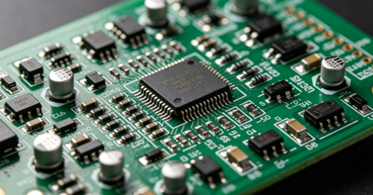
SMDs come in a wide variety of shapes, sizes, and configurations, each tailored to specific functions within a circuit. Common types of SMDs include resistors, capacitors, diodes, transistors, integrated circuits (ICs), and sensors. Unlike through-hole components, which have long leads that pass through drilled holes in the PCB and are soldered on the opposite side, SMDs feature either short leads, solder pads, or no leads at all, allowing them to be attached directly to the PCB surface. This design makes SMDs significantly smaller and lighter than their through-hole counterparts, a critical advantage in the era of miniaturized electronics.
The miniaturization of SMDs has revolutionized the electronics industry, enabling the creation of sleek, compact devices without compromising performance. For example, a smartphone may contain thousands of tiny SMD resistors and capacitors, alongside larger SMD ICs, all packed into a slim casing. In PCB assembly, the selection of SMDs depends on factors such as the device’s functional requirements, size constraints, power needs, and environmental conditions (e.g., temperature, humidity, and vibration resistance).

Surface Mount Technology (SMT): The “Assembly Method” for SMDs
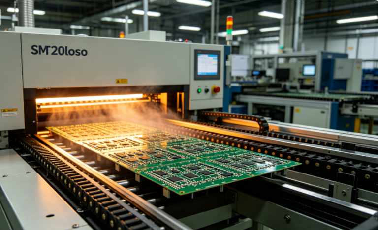
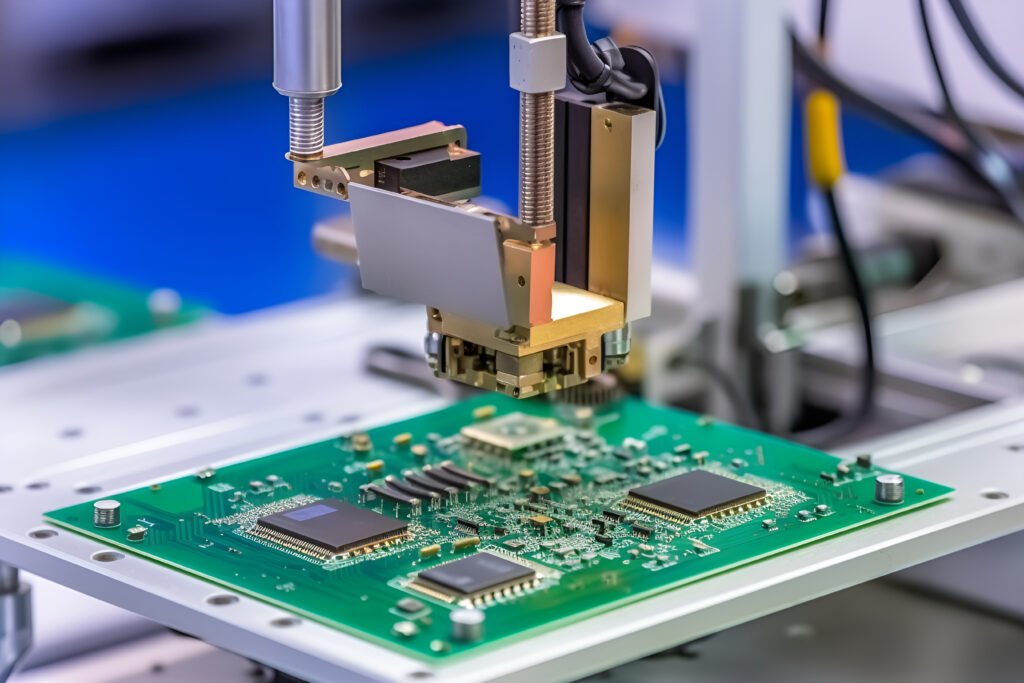
SMT, or Surface Mount Technology, is the automated manufacturing process used to place, align, and solder SMDs onto the surface of a PCB. It is the primary assembly method for modern PCBs, replacing the older through-hole technology (THT) in most applications due to its efficiency, precision, and suitability for high-volume production. SMT is not a component itself; rather, it is a set of techniques, equipment, and procedures that enable the reliable assembly of SMDs onto PCBs.
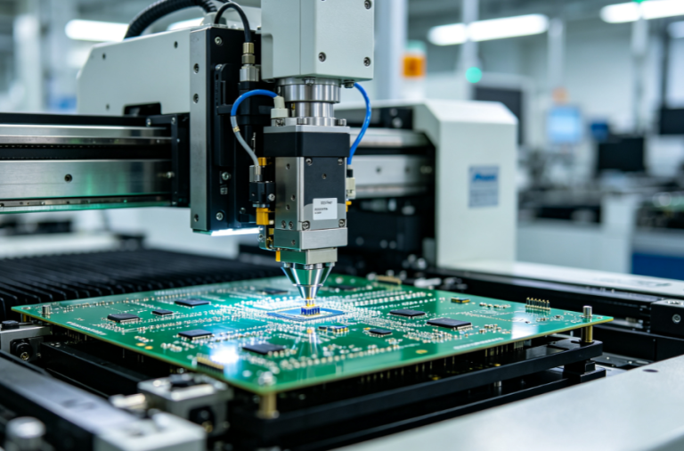
The SMT assembly process typically involves several key steps, all of which are highly automated to ensure consistency and accuracy. First, solder paste—a mixture of tiny solder particles and flux—is applied to the designated solder pads on the PCB surface using a stencil printer. The stencil is a thin metal sheet with cutouts matching the shape and position of the SMDs, ensuring that solder paste is applied only where needed. Next, a pick-and-place machine, equipped with robotic arms and vacuum nozzles, picks up individual SMDs from their packaging (usually tape-and-reel or trays) and places them precisely onto the solder pads with micron-level accuracy. After placement, the PCB is passed through a reflow oven, where it is heated in a controlled temperature profile to melt the solder paste, creating a permanent electrical and mechanical bond between the SMDs and the PCB. Finally, the assembled PCB undergoes inspection and testing to identify any defects, such as misaligned components, cold solder joints, or short circuits.
SMT has become the industry standard for PCB assembly because it offers numerous benefits over THT. It allows for higher component density, meaning more components can be placed on a single PCB, which is essential for compact devices. It also enables faster production speeds, lower labor costs (due to automation), and improved electrical performance, as the shorter connections between SMDs reduce signal resistance and inductance. Additionally, SMT is more compatible with modern manufacturing techniques, such as automated optical inspection (AOI) and X-ray inspection, which ensure the quality of the assembled PCBs.
How SMD and SMT Work Together

The relationship between SMD and SMT is one of interdependence—they are inseparable in modern PCB assembly, and neither can fulfill its purpose without the other. Simply put, SMDs are the components that need to be assembled, and SMT is the process that assembles them. This symbiotic relationship is what drives the efficiency and innovation of today’s electronics manufacturing.
First and foremost, SMDs are specifically designed to be compatible with SMT. Their compact size, surface-mountable design, and standardized solder pads are all optimized for the automated placement and soldering processes of SMT. Without SMDs, SMT would have no components to assemble, and the technology would be irrelevant. Conversely, without SMT, SMDs could not be efficiently or reliably mounted onto PCBs in high volumes. While it is technically possible to hand-solder small quantities of SMDs, this method is slow, prone to human error, and impractical for mass production—exactly the scenario that SMT was developed to address.
The evolution of SMDs and SMT has also been closely linked. As electronics manufacturers demanded smaller, more powerful devices, SMD designers created increasingly miniaturized components, which in turn required advancements in SMT equipment to handle their tiny size and precise placement needs. For example, the development of ultra-small SMDs (such as 01005 resistors and capacitors, which measure just 0.4mm x 0.2mm) required pick-and-place machines with higher precision and more advanced vision systems to ensure accurate placement. Similarly, the introduction of complex SMDs like ball grid arrays (BGAs) and chip scale packages (CSPs) led to the adoption of X-ray inspection in SMT, as these components have hidden solder joints that cannot be seen with traditional optical inspection.
In PCB assembly, the choice of SMDs directly influences the SMT process, and vice versa. For instance, larger SMDs (such as power ICs) may require a different solder paste application process or a modified reflow temperature profile to ensure proper soldering. Conversely, the capabilities of a manufacturer’s SMT equipment (e.g., the precision of the pick-and-place machine, the size of the reflow oven) will determine the types of SMDs that can be used in a PCB design. At our PCB assembly facility, we have invested in state-of-the-art SMT equipment that can handle a wide range of SMD sizes and types, from the smallest 01005 components to large BGAs and QFNs (Quad Flat No-leads packages), ensuring that we can meet the diverse needs of our clients.

Key Differences: SMD vs. SMT
While SMD and SMT are closely connected, they are fundamentally different in their nature, purpose, and characteristics. To avoid confusion, it is important to clearly distinguish between the two, as each plays a unique role in PCB assembly. The following table summarizes the key differences, followed by a detailed explanation of each point.

1. Nature: Component vs. Process

The most fundamental difference between SMD and SMT is their nature. SMDs are physical, tangible components that make up the circuitry of a PCB. They are the “parts” that you can hold, see, and install (or have installed) onto the board. Examples include a tiny 0402 resistor, a microchip IC, or a surface-mount diode. Each SMD has a specific electrical function, and its performance is determined by its design, materials, and specifications.
In contrast, SMT is an intangible process—a set of steps and techniques used to assemble those components onto the PCB. It does not have a physical form; instead, it is implemented using specialized equipment (stencil printers, pick-and-place machines, reflow ovens) and controlled by software and engineering protocols. SMT is about how components are placed and soldered, not what components are used.

2. Purpose: Functional vs. Assembly

SMDs are designed to perform specific electrical functions within a circuit. A resistor regulates current flow, a capacitor stores electrical charge, a transistor amplifies signals, and an IC integrates multiple electronic functions into a single chip. The selection of SMDs is driven by the functional requirements of the electronic device—for example, a high-power industrial device may require SMDs with higher voltage and current ratings, while a portable consumer device may prioritize small, low-power SMDs.
SMT, on the other hand, is designed to solve the challenge of assembling SMDs onto PCBs efficiently, accurately, and at scale. Its purpose is not to perform any electrical function but to ensure that SMDs are mounted correctly, securely, and with reliable electrical connections. The goal of SMT is to minimize defects, maximize production speed, and reduce costs—all while maintaining the quality and performance of the assembled PCB.

3. Form: Tangible vs. Procedural

As mentioned earlier, SMDs are physical objects with distinct shapes and sizes. They come in standardized packages, such as 01005, 0402, 0603 for passive components (resistors, capacitors), and SOP (Small Outline Package), QFP (Quad Flat Package), BGA for ICs. Each package type has specific dimensions and solder pad requirements, which must be matched to the PCB design and SMT process.
SMT, by contrast, is a procedural form—it consists of a sequence of steps that must be followed in a specific order to achieve successful assembly. These steps include solder paste printing, component placement, reflow soldering, and inspection/testing. Each step requires specialized equipment and skilled technicians to monitor and optimize the process. For example, the reflow soldering step requires precise control of temperature and time to ensure that the solder paste melts properly, wets the solder pads and SMD leads, and forms a strong, reliable joint without damaging the components.

4. Customization: Component Selection vs. Process Optimization

Customization for SMDs involves selecting the right components for the circuit design. This includes choosing the correct type of SMD (e.g., a ceramic capacitor vs. a tantalum capacitor), the appropriate specifications (e.g., a 10kΩ resistor vs. a 100kΩ resistor), and the right package size (e.g., 0402 vs. 0603) based on factors like space constraints, power requirements, and cost. At our PCB assembly service, we work closely with clients to select the optimal SMDs for their projects, ensuring that they meet both functional and budgetary needs.
Customization for SMT involves optimizing the assembly process to fit the specific requirements of the PCB design, SMD types, and production volume. This may include adjusting the stencil design to ensure proper solder paste application for different SMD sizes, modifying the reflow temperature profile to accommodate heat-sensitive components, or selecting the right pick-and-place nozzles for small or irregularly shaped SMDs. For high-volume production, we may also optimize the SMT process for speed, while for low-volume, high-precision projects, we focus on maximizing accuracy and minimizing defects.

5. Failure Modes: Component Defects vs. Process Errors
SMD failures are typically caused by component defects or damage. This can include manufacturing defects in the SMD itself (e.g., a faulty IC chip, a resistor with the wrong resistance value), physical damage during handling or assembly (e.g., a cracked capacitor, bent leads), or environmental factors (e.g., overheating due to excessive current, corrosion from humidity). In some cases, SMD failures can also be caused by improper soldering (e.g., a solder joint that does not make good electrical contact), but this is a result of a flawed SMT process rather than an SMD defect.
SMT failures, by contrast, are caused by errors in the assembly process. Common SMT defects include misaligned components (where an SMD is placed off-center on the solder pads), cold solder joints (where the solder did not melt properly, resulting in a weak or non-conductive joint), solder bridges (where excess solder connects two adjacent solder pads, causing a short circuit), and tombstoning (where a small SMD, such as a resistor or diode, stands on end instead of lying flat on the PCB). These defects can be minimized through proper process optimization, regular equipment maintenance, and rigorous inspection.
Practical Applications: SMD and SMT in PCB Assembly
To illustrate the real-world relationship and differences between SMD and SMT, let’s consider a practical example: the assembly of a PCB for a smartwatch. Smartwatches require compact, lightweight, and low-power PCBs, making SMDs and SMT the ideal choice.
First, the PCB design will specify a range of SMDs tailored to the smartwatch’s functions. These will include tiny 01005 resistors and capacitors to regulate power and signal flow, a small microcontroller IC (in a BGA or QFN package) to handle processing, a surface-mount battery connector, a touch sensor SMD, and a display driver IC. Each of these SMDs is selected for its small size, low power consumption, and ability to perform its specific function reliably.
Next, the SMT process is used to assemble these SMDs onto the PCB. Solder paste is printed onto the PCB’s solder pads using a precision stencil, ensuring that only the required amount of solder is applied. A high-precision pick-and-place machine then places each SMD onto its designated position, with micron-level accuracy to avoid misalignment. The PCB is then passed through a reflow oven with a temperature profile optimized for the heat-sensitive SMDs (such as the microcontroller and touch sensor), melting the solder paste and creating strong electrical and mechanical bonds. Finally, the assembled PCB is inspected using automated optical inspection (AOI) to check for defects like misplacement or solder bridges, followed by functional testing to ensure that all SMDs are working correctly together.
In this example, the SMDs are the “building blocks” that enable the smartwatch’s functionality, while the SMT process is the “construction method” that assembles these blocks into a working PCB. Without the compact SMDs, the smartwatch could not be as small and lightweight as it is, and without the precise SMT process, the SMDs could not be assembled efficiently or reliably.
Another example is the assembly of a PCB for an industrial control system. These systems require PCBs that are durable, reliable, and capable of operating in harsh environments (e.g., high temperatures, vibration). For this application, we would select SMDs with high temperature ratings and robust packaging (e.g., metal-core SMDs for power components). The SMT process would be optimized for reliability, with additional steps such as conformal coating (to protect the PCB and SMDs from moisture and corrosion) and X-ray inspection (to check the solder joints of complex SMDs like BGAs). Again, the SMDs are chosen for their functional and environmental suitability, while the SMT process is tailored to ensure the PCB’s durability and reliability.
Our Expertise in SMD and SMT for PCB Assembly

At Ucreate, we specialize in PCB manufacturing and PCB assembly, with extensive expertise in both SMDs and SMT. Our state-of-the-art facility is equipped with the latest SMT equipment, including high-precision pick-and-place machines, advanced reflow ovens, and automated inspection systems (AOI and X-ray), enabling us to handle a wide range of SMD sizes and types, from the smallest 01005 components to large, complex BGAs and QFNs.
Our team of experienced engineers and technicians works closely with clients to select the optimal SMDs for their projects, ensuring that they meet functional, performance, and budgetary requirements. We also optimize the SMT process for each project, adjusting parameters like solder paste application, component placement, and reflow temperature to minimize defects and maximize efficiency. Whether you need prototype PCBs with a small number of SMDs or high-volume production runs with thousands of components, we have the capabilities and expertise to deliver high-quality results on time and on budget.
We understand that every PCB assembly project is unique, and we take a customized approach to meet your specific needs. Our quality control processes are rigorous, with multiple inspection and testing steps to ensure that every PCB we produce is reliable, functional, and meets industry standards. We also offer additional services such as conformal coating, component sourcing, and functional testing, providing a comprehensive solution for all your PCB assembly needs.

Conclusion
SMD and SMT are two core concepts in modern PCB assembly, working together to power the electronic devices that shape our daily lives. SMDs are the physical components that perform electrical functions, while SMT is the automated process that assembles these components onto PCBs efficiently and accurately. While they are closely connected, they are fundamentally different in their nature, purpose, and characteristics, and understanding these differences is essential for making informed decisions in PCB assembly.
Whether you are designing a compact consumer device, a rugged industrial system, or anything in between, the right combination of SMDs and SMT is key to achieving a reliable, cost-effective, and high-performance PCB. At [Your Company Name], we are committed to helping you navigate the complexities of SMD and SMT, providing expert guidance, high-quality components, and state-of-the-art assembly services to bring your electronic projects to life. Contact us today to learn more about how we can support your PCB and PCB assembly needs.

We Provide High-end Quality Rigid PCB, Flexible PCB, Rigid-flex PCB, Metal Core PCB; 2-64L Mutilayer PCB; HDI PCB (2+N+2); High Frequency PCB Manufacturing and Assembly.

Sen your Gerber file or BOM list for free quote:
Email:  sales@ucpcba.com
Whatsapp: +8613798955467

We'd love to hear from you! We will reply within 2 hours.

Upload ( Allowed File Types .zip .rar .doc .docx .jpg .xls... )