
 English
 中文
中文In the ever-evolving landscape of semiconductor packaging, Ball Grid Array (BGA) technology stands as a cornerstone of modern electronics manufacturing. Whether you’re designing high-performance computing systems, mobile devices, or automotive electronics, mastering BGA package design is essential for achieving optimal performance, reliability, and manufacturability. This comprehensive guide will walk you through the critical aspects of BGA package design, equipping you with the knowledge to create robust, high-yielding products.
Understanding the Fundamentals of BGA Architecture
Before diving into the design specifics, it’s crucial to understand what makes BGA technology so prevalent in today’s electronics industry. Unlike traditional leaded packages such as Quad Flat Packages (QFP), BGA packages utilize an array of solder balls on the bottom surface for electrical and mechanical connection to the printed circuit board (PCB). This configuration offers numerous advantages including higher pin counts, improved electrical performance, better thermal characteristics, and enhanced mechanical reliability.
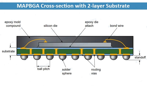
The cross-sectional view above illustrates the typical structure of a Mold Array Process BGA (MAPBGA). As you can see, the package consists of several critical layers: the silicon die, die attach material, bond wires connecting the die to the substrate, the multi-layer substrate itself, solder mask, and finally the solder balls that interface with the PCB. Understanding this layered architecture is fundamental to successful design implementation.
Critical Design Parameters: Pitch, Ball Diameter, and Land Patterns
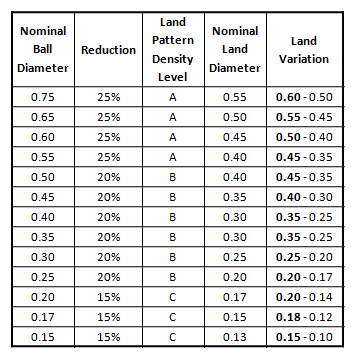
The table above provides essential guidelines for land pad diameter selection based on nominal ball diameter. Notice how land pattern density levels (A, B, C) affect the recommended dimensions. Level A represents the most robust design with maximum copper area, suitable for high-reliability applications, while Level C offers the highest density for space-constrained designs. Your selection should balance manufacturing yield, reliability requirements, and board real estate constraints.
Substrate Design: The Hidden Complexity
The substrate serves as the critical bridge between the silicon die and the PCB, and its design requires careful consideration of multiple factors. Modern BGA substrates are typically multi-layer organic structures with 2 to 6+ layers, each serving specific routing and power distribution functions.
- Dedicated power and ground planes to reduce loop inductance
- Strategic placement of decoupling capacitor pads near power/ground ball clusters
- Via stitching patterns that optimize current flow while maintaining signal integrity
Thermal Management: Keeping Your Cool
Thermal performance can make or break a BGA design, particularly for high-power applications such as processors, FPGAs, and power management ICs. The BGA format offers inherent thermal advantages through the solder ball array, which provides multiple thermal paths to the PCB ground planes.
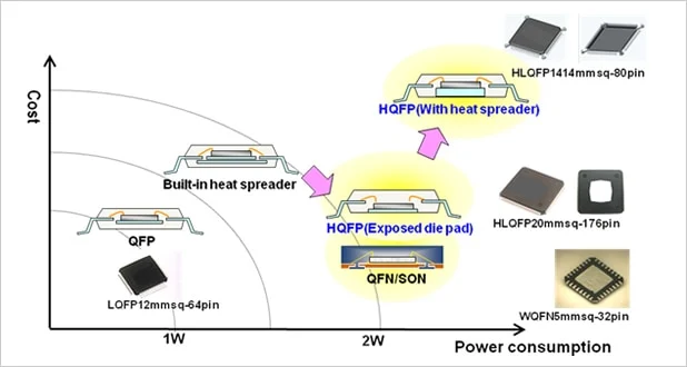
The thermal hierarchy diagram above illustrates how different package types compare in thermal performance. Standard BGAs provide baseline thermal capability, while enhanced versions incorporate thermal balls, exposed pads, or integrated heat spreaders for demanding applications.
- Thermal Ball Arrays: Implement a central grid of solder balls dedicated to thermal conduction rather than electrical signals. These balls connect directly to PCB ground planes, creating efficient heat dissipation paths.
- Exposed Pad (EP) Designs: Many modern BGA variants feature a central exposed metal pad on the package bottom. This pad solders directly to a thermal land on the PCB, significantly improving thermal conductivity compared to standard ball connections.
- Substrate Material Selection: High thermal conductivity substrate materials, such as those with ceramic fillers or metal cores, can improve thermal performance by 20-40% compared to standard FR-4 based substrates.
- Mold Compound Properties: Select mold compounds with high thermal conductivity (>1.0 W/mK) for power-dense applications, ensuring efficient heat spreading from the die surface.
A BGA package cannot succeed in isolation—it must harmonize with the PCB design. The layout phase requires careful coordination between package substrate design and board-level routing constraints.
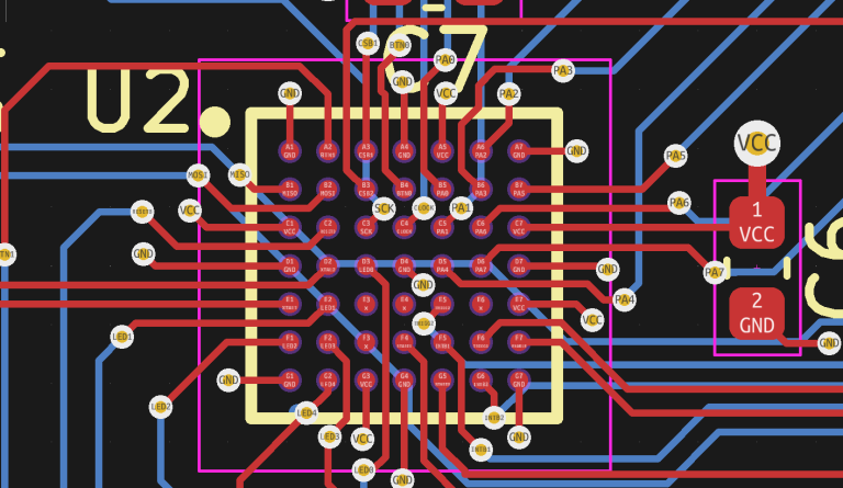
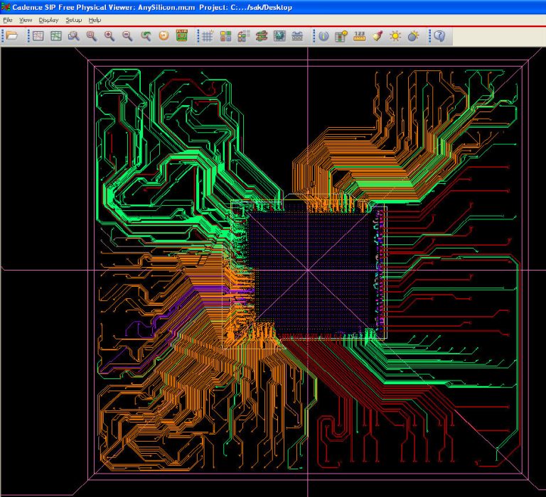
The layout example above demonstrates a typical BGA fan-out pattern. Notice the systematic approach to trace routing: outer rows escape on the surface layer, while inner rows utilize vias to access deeper layers. This “via channel” approach maximizes routing density while maintaining manufacturability.
Critical PCB layout guidelines include:
- Via Size and Placement: Use microvias (0.1mm-0.15mm drill) for high-density designs, ensuring adequate annular ring (minimum 0.05mm) for reliability. Position vias on a grid that aligns with your BGA ball pattern to maximize routing channels.
- Solder Mask Design: Implement solder mask defined (SMD) pads for fine-pitch BGAs to improve solder joint co-planarity. The solder mask opening should be 0.05mm to 0.1mm smaller than the copper pad diameter to prevent solder bridging.
- Component Keep-Out Zones: Maintain adequate clearance around the BGA for rework equipment access. Typically, allow 3-5mm clearance from the package edge for hot-air rework nozzles.
- Thermal Relief Patterns: For thermal balls and exposed pads, use thermal relief patterns that balance soldering manufacturability with thermal performance. Solid connections offer better thermal conductivity but may cause soldering issues due to heat sinking.
Signal Integrity and Power Delivery Network Design
High-speed BGA designs demand rigorous attention to signal integrity (SI) and power delivery network (PDN) performance. The transition from the die through the substrate, solder balls, and PCB creates multiple impedance discontinuities that must be managed.
- Controlled Impedance Routing: Maintain consistent trace impedance (typically 50Ω single-ended, 100Ω differential) throughout the signal path. Account for the impedance reduction caused by closely spaced BGA balls by adjusting trace widths in the breakout region.
- Via Optimization: Minimize via stub length by using blind or buried vias where possible. For through-hole vias in high-speed paths, consider back-drilling to remove unused via barrel sections that create resonant stubs.
- Length Matching: For parallel bus interfaces, implement length matching within the BGA breakout region. Modern high-speed interfaces (DDR4/5, PCIe Gen4/5) require tight length tolerances (±5mil or better) that must be maintained from die to connector.
- Decoupling Strategy: Place high-frequency decoupling capacitors as close as possible to power/ground ball pairs. For high-power BGAs, consider embedded capacitance layers in the substrate or PCB to provide ultra-low inductance decoupling.
- Current Density: Calculate current density in power vias and traces to ensure they remain within safe limits (typically <10A/mm² for long-term reliability). High-current paths may require multiple parallel vias or wider traces.
Manufacturing and Assembly Considerations
Even the most elegant BGA design fails if it cannot be manufactured reliably. Design for Manufacturing (DFM) and Design for Assembly (DFA) principles must guide your decisions throughout the design process.
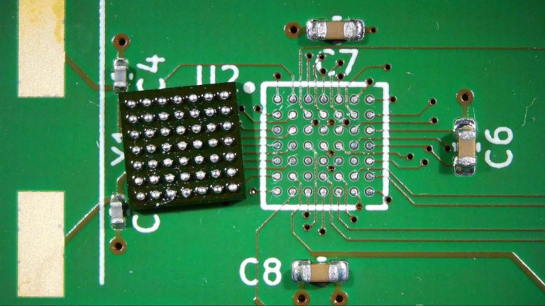
The image above shows BGA packages during assembly and rework operations. Notice the precise ball placement and the importance of proper solder joint formation.


