
 English
 中文
中文1. What is uneven PCB etching?
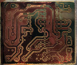
In PCB manufacturing, etching is a critical step in dissolving the copper layer by chemical potions (e.g., acidic copper chloride solution) to form a conductive line.Uneven etching refers to the line copper layer is etched at an inconsistent rate or depth, resulting in deviations in line width and thickness.
Pool effect is a typical manifestation of uneven etching – etching solution in the PCB surface local accumulation (like a “puddle”), resulting in excessive etching in the region (line thinning or even circuit breakers) or insufficient (line residual excessive short-circuit), which directly affects the performance of the circuitand yield.
2. Causes of the pool effect: why do liquids "puddle"?
PCB etching uneven core reason is the etching solution in the plate surface flow is not smooth, specific performance:
- Board structure “depression” more:
PCB line design, high-density lines, small gaps (such as line width / line spacing <5mil) or blind holes / buried holes around the formation of “low-lying areas”, etching solution is easy to stagnate. - Uneven spray coverage:
Etchers spray etchant at high pressure onto the board surface through a spray nozzle.If the nozzles are clogged, the pressure is insufficient, or the layout is not reasonable, it will lead to insufficient coverage of some areas of the chemical water, while other areas of the chemical water build-up. - Board warping or loose clamping:
PCB in the etching conveyor belt if warping (such as due to temperature changes), or clamping device is not pressed edge, will lead to the board and the spray direction of the angle of the anomalies, the potion is more likely to be in the local stagnation. - Etching fluid characteristics impact:
etching fluid viscosity, surface tension is too high (such as too much additives) will reduce the mobility, exacerbate the accumulation; uneven temperature can also lead to local reaction rate differences.
3. The dangers of the pool effect: from line to yield
The pooling effect directly causes the PCB line geometry to deviate from the design values, leading to multiple problems:
- Excessively thin or broken lines: Over-etched areas where the copper layer is excessively dissolved and signal transmission is interrupted.
- Excessive line residue: Insufficiently etched areas where the copper layer is not completely removed, resulting in short circuits between lines.
- Impedance mismatch: Uneven line widths can change signal transmission impedance, affecting the performance of high-frequency circuits (e.g., 5G communication boards).
- Decreased yield: Additional optical inspection, rework, or scrap is required, significantly increasing production costs.
4. Solution: How to make the etchant "flow"?
① Optimisation of etching machine design and process parameters
- Spraying system upgrade:
adopts high-pressure spraying (pressure ≥30psi) and multi-angle nozzle layout (e.g., upper and lower double-sided spraying) to ensure that there is no dead angle of the liquid coverage; clean the nozzles regularly to avoid clogging. - Increase plate surface disturbance:
Set up ultrasonic vibration or airflow stirring device in the etching tank to break the surface tension of etching liquid and promote liquid flow. - Control etching speed matching:
Adjust the spraying speed and conveyor speed (such as reducing the conveyor speed to extend the etching time), to avoid too fast to cause the potion is not fully effective.
② improve PCB design and manufacturing process
- Layout optimisation:
Avoid concentrated design of high-density lines and increase line spacing (e.g. ≥8mil); make “etching compensation” around blind/embedded holes (appropriately widen the copper layer at the edge of the holes). - Board pre-treatment:
Bake the PCB before etching (e.g. 120℃×30min) to reduce the warping caused by internal stress; use vacuum clamping or edge fixing device to ensure that the board surface is flat.
③ Environment and potion management
- Real-time monitoring of potion parameters:
Control the etchant temperature (e.g. 25±1°C), concentration (e.g. Cu²⁺concentration ≤ 120g/L) and pH to avoid viscosity increase due to aging of the potion. - Regular replacement of the potion:
Replace the etching solution regularly according to the production volume (e.g. every 8 hours) to prevent the accumulation of impurities affecting the fluidity.
5. Summary
The pool effect of uneven PCB etching is the result of multi-factor coupling of design, equipment and process.By optimising the etching machine spray and flow design, improving the PCB line layout, and strictly controlling the parameters of the potion, we can effectively reduce the problem of uneven etching, improve the conductivity and yield of PCB, and meet the manufacturing needs of high-precision electronic products.


