
 English
 中文
中文Circuit boards are made up of layers of copper foil circuitry, and the connection between different circuit layers relies on these ‘via’ holes. This is because today’s circuit boards are made using drilled holes to connect between different circuit layers, just like the connection of multi-layer underground water pipes. The difference is that the water pipe is to allow the water to flow, while the purpose of the circuit board connection is for the electrical characteristics can conduct electricity, so it is called the conductive holes, but if you just use a drilling machine or laser drilled holes will not conduct electricity, so it is necessary to drill the holes in the surface of a layer of conductive material plating (usually ‘copper’), so that the electrons can move between the different layers of copper foil, because the original drilled holes in the surface of the only resin will not be This is so that electrons can move between the different layers of copper foil.
In general, we often see the there are three kinds of PCB hole (Via) , are described as follows:
Plating Through Hole (PTH)
This is the most common type of through-hole, you just need to hold the PCB up to the light, you can see the bright hole is ‘through-hole’. This is also the simplest type of through-hole because it is cheaper to just use a drill or laser to drill all the holes directly into the board. But relatively, some circuit layers do not need to connect these through-holes, for example, we have a six-storey house, working bears rich, bought its third and fourth floors, and then, working bears themselves in the third and fourth floors between the design of a staircase connected to each other, and the working bears do not need to connect to the other floors, at this time, if you design another staircase through the one to six floors of each floor, which will form a Waste, with the current circuit board inch, should not be allowed. So although through-hole is cheaper, sometimes it will use up more space on the PCB.
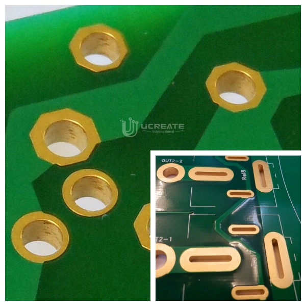
Blind Via Hole
Blind vias are used to connect the outermost circuit layer of a PCB to the neighbouring inner layer by plating holes that do not go through, as they cannot be seen from the other side. In order to increase the space utilisation of PCB circuit layers, the ‘blind hole’ process was developed. This method requires special attention to the depth (Z axis) of the drilled holes, but this method often causes difficulties in plating the holes, so it is almost no longer used by manufacturers.
It is also possible to drill holes for the circuit layers that need to be connected at the time of individual circuit layers, and then glue them together at the end, for example, 2+4+2, you can drill holes to connect the two outermost layers first, or connect the 2+4 boards at the same time, but this requires a more precise positioning and alignment device.
Taking the above example of buying a flat, in a six-storey house, only the staircase connecting the first and first floors, or the staircase connecting the fifth floor to the sixth floor, is called a blind hole.
A ‘blind hole’ is a hole that can be seen from one side of the board, but not the other.

Buried Via Hole
Any circuit layer inside the PCB is connected but not connected to the outer layer. This process cannot be achieved by bonding and then drilling, but must be drilled at the time of individual circuit layers, first partially bonded to the inner layer and then electroplated, and finally bonded to all, more laborious than the original ‘through-hole’ and ‘blind hole’, and therefore the most expensive. This process is usually only used in high density (HDI) circuit boards to increase the space available for other circuit layers. Take the above example of buying a flat, a six-storey house only has a staircase connecting the third and fourth floors, which is called a buried hole.
A ‘buried hole’ is a hole that is not visible from the outside of the board, but is actually buried in the inner layer of the board.
Ucreate PCB engineers have more than 10 years in electronic industry. We can provide standar technology as well as all your special needs.
Send your Gerber file to sales@ucpcba.com, we can offer you the free DFAM check fristly.


