
 English
 中文
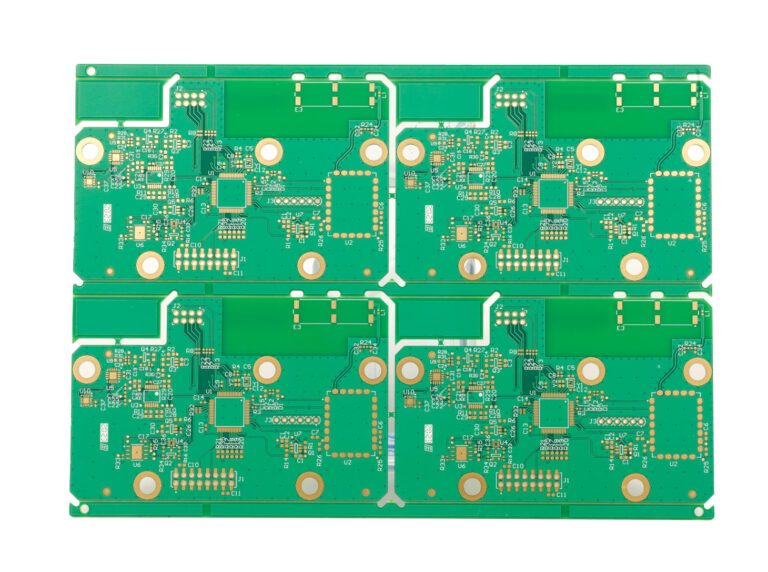
中文Circuit board, also known as printed circuit board (PCB), is an electronic basic device, mainly used for building and arranging circuit components with circuit diagram. It is usually composed of multiple layers of material, including, but not limited to, metal, plastic, insulation, and control layers. Between these layers, there will be perforated and plated conductor sections for connection and conduction. The core role of circuit boards is to make the circuits miniature and intuitive, which is crucial for the mass production of fixed circuits and the large-scale optimization of the layout of electrical appliances.
The working principle of the circuit board is to use printing technology and electronic components, print circuit patterns on its surface and install electronic components, such as integrated circuits, resistance, capacitors, inductors, etc., to realize the function of electronic products. These circuit patterns are usually copper foil patterns that are made by etching, adding printing ink, or repeating the patterns. Their high wiring density, low weight, thin thickness, and good bending properties make circuit boards ideal for electronic devices.
Compatible design
Electromagnetic compatibility (EMC) refers to the ability of electronic equipment to function effectively in different electromagnetic environments. The goal is to ensure that the equipment can both suppress external interference and operate normally in a specific electromagnetic environment, while also minimizing the equipment’s own electromagnetic interference on other devices.
1. When designing a PCB circuit board, it is important to select an appropriate wire width to minimize the impact of transient current interference on the printed lines. This interference is primarily caused by the inductance of the printed wire, so it is important to reduce the wire’s inductance as much as possible.
2. Using the correct wiring strategy with equal wiring can reduce wire inductance. However, it can also increase the mutual sense between wires and the distribution of capacitance. If the layout allows, the best approach is to use a well-shaped mesh wiring structure. A concrete way to achieve this is to have lateral side wiring on one side of the printed board and longitudinal wiring on the other side. Then, use metal holes in the cross holes.
3. To prevent crosstalk between PCB circuit board wires, it is important to avoid long distance equal wiring during the design and wiring process. The distance between lines should be maximized, and signal lines, ground lines, and power lines should not intersect whenever possible. To effectively inhibit crosstalk, a grounded printed line can be added between sensitive signal lines.
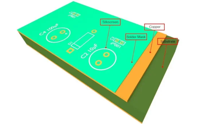
Constitute
The circuit board is mainly composed of welding pad, through hole, installation hole, conductor, components, connectors, filling, electrical boundary, etc. The main functions of each component are as follows:
Pad: metal holes for welding pins of components.
Over holes: there are metal holes and non-metal holes, in which the metal holes are used to connect the component pin between the layers.
Installation hole: for fixing the circuit board.
Lead: electrical network copper film for connecting component pins.
Connector: components for connection between circuit boards.
Fill: copper application for ground network can effectively reduce the impedance.
Electrical boundary: used to determine the size of the circuit board, all components on the circuit board cannot exceed the boundary
The primary categorisation
- The circuit board is classified into single-sided PCBs, double-sided PCBs, and multi-layer circuit boards.
Single-Sided Boards
A single-sided PCB has all the components on one side and the wires on the other. This type of PCB is simple to make and cost-effective. However, it is not suitable for complex products.
Double-Sided Boards
This circuit board has wiring on both sides. However, to utilize both sides, a proper circuit connection between them is necessary. This connection is called the guide hole (via), which is a small hole filled or coated with metal that can be used to connect wires on both sides. The dual panel is better suited to more complex circuits than a single panel due to its larger size and the ability to stagger the wiring to the other side.
Multilayer boards
A multilayer board is a printed board with more than three layers of conductive graphics and insulation material. The conductive graphics are interconnected according to specific requirements. Multi-layer circuit boards are products of electronic information technology that aim for high speed, multi-functionality, large capacity, small volume, thin shape, and lightweight design.
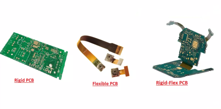
2. Additionally, the circuit board can be classified into flex PCB (FPC), rigid PCB, and rigid-flex PCB (R-F PCB).
FPC, or Flexible Printed Circuit, is a highly reliable printed circuit board with good wiring density and flexibility. It is based on a flexible insulating substrate, such as polyimide or polyester film, that can be bent, rolled, and folded to suit different designs and needs. Flexible circuit boards have the ability to integrate numerous precision components in a limited space while also being able to move and stretch in three dimensions. This allows for the integration of component assembly and wire connections. They are commonly used in mobile phones, computers, and other portable electronic devices, reducing the size and weight of electronic products while improving their flexibility and reliability.
Rigid PCB
Generally, FR 4 is used as a substrate. It cannot be bent or scratched and is often used in applications that do not require flexibility but require high strength.
Rigid-flex PCB (R-F PCB)
The combination of flexible circuit boards and rigid circuit boards through compression
gave birth to the new product of soft and hard combination boards, which possess both FPC and PCB characteristics. Therefore, after the pressing and closing processes, the circuit board is formed according to the relevant process requirements.
Work level
Circuit board includes many types of working levels, such as signal layer, protective layer, screen printing layer, internal layer, etc. The role of various levels is briefly introduced as follows:
(1) Signal layer: mainly used to place components or wiring. Protel DXP Usually contains 30 intermediate layers, namely Mid Layer1~Mid Layer30. The intermediate layer is used to arrange signal lines, and the top and bottom layers are used to place components or apply copper.
(2)Protective layer: mainly used to ensure that the circuit board does not need tin plating place is not tin, so as to ensure the reliability of the circuit board operation. Where Top Paste and Bottom Paste are top and bottom weld resistance layer respectively; Top Solder and Bottom Solder are tin paste protection layer and bottom layer respectively.
(3)Silk printing layer: mainly used to print the serial number of components, the production number and the company name on the circuit board.
(4)Internal layer: mainly used as a signal wiring layer, Protel DXP contains a total of 16 internal layers
(5)Other layers: mainly including 4 types of layers:
- Drill Guide:Mainly used for the location of drilling on printed circuit boards.
- Keep-Out Layer:Mainly used to draw the electrical frame of the circuit boards.
- Drill Drawing:Mainly used to set the drilling shape.
- Multi-Layer:Mainly used to setting multi-faceted layers.
PCB making technology
The technology used in making PCB boards includes computer-aided manufacturing (CAD/CAM) processing and light painting technology. The technology used in making PCB boards includes computer-aided manufacturing (CAD/CAM) processing and light painting technology. The given text already meets the desired characteristics of clarity, conciseness, precision, and grammatical correctness. Therefore, no changes were made to the original text.
Computer-aided manufacturing (CAM) is based on various processes. To meet the process requirements mentioned above, certain preparations must be made before light painting. These preparations include addressing issues such as mirror imaging, welding resistance expansion, process line, process frame, line width adjustment, center hole, shape line, and other related concerns.
Complete this process carefully. Note that the user file has limited space and must be handled accordingly. Due to variations in process and technical level among factories, adjustments may be necessary in production to meet user requirements.
Precision and other requirements are essential in CAM processing, which is a crucial step in modern printed circuit manufacturing.
Work done by the CAM
⒈ Plate size correction, combined with D code.
⒉ Correct the line width, and combine the D code.
⒊ Check the minimum spacing, between the pad and pad, between the pan and lines, between lines and lines.
⒋ Aore size inspection, combined.
⒌ Check of the minimum linewidth.
⒍ Determine the welding expansion parameters.
⒎ performed the mirror image.
⒏ Add various process lines, process frames.
⒐ Line width correction for correcting side erosion.
⒑ Form the central hole.
⒒ Add profile corners.
⒓ Plus positioning hole.
⒔ Plate and plate, rotation, mirror image.
⒕ Spellings.
⒖ Superposition processing of graphics, tangent processing.
⒗ Add a user’s trademark.


