
 English
 中文
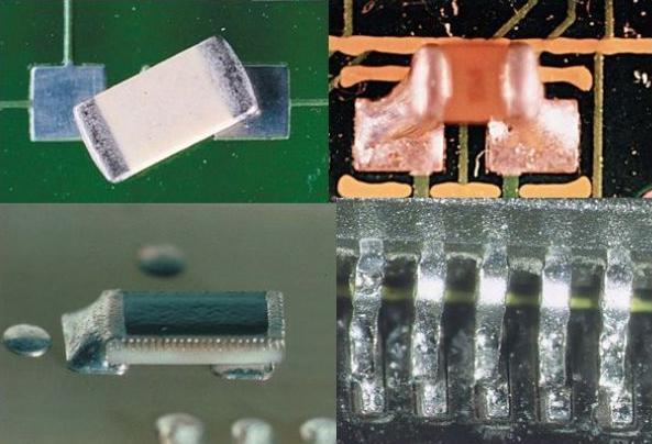
中文Do you encounter plug-in components that won’t plug in? Do you encounter plug-in components that do not go in? Solder joints that are white, weak, or fall off frequently? Or the circuit is sometimes good and sometimes bad but can not find the reason? It may be a problem of poor soldering – poor soldering is a common problem in electronic production, poor soldering is known as electronic production in the ‘persistent disease’, and the PCB Pad and Hole size design is not reasonable, is often the key to this problem! ‘fuse’. Once the Pad and Hole size design is not proper, welding bad condition will occur frequently, components may appear displacement, false welding, side stand or even can not be normal welding and other phenomena, which seriously affects the performance of the entire circuit, resulting in unstable function of the product, malfunctioning, or even completely failed, to the electronic production to bring a great deal of trouble.
I.Common problems with pads leading to poor soldering
Pad Overlap
In multilayer pcb design, pad overlap can lead to drill bit breakage or hole damage during drilling.This is due to inaccurate positioning of the overlapping pads during the drilling operation and uneven force applied to the drill bit.This not only damages the drill bit, but may also prevent the pads from functioning properly, leading to product scrap.
For example, on complex circuit boards, if the critical signal pads of different layers overlap, problems are highly likely to occur when drilling, affecting the soldering of subsequent components.
Inconsistent pad sizes
Inconsistent pad sizes can result in uneven pulling forces, which can lead to problems such as device displacement and empty soldering.When the size of the pads are different, the flow and adhesion of the solder during soldering is different, which has a great impact on the fixing and electrical connection of the components.For example, in the SMT patch, different sizes of pads will make the components uneven force, easy to produce the phenomenon of bias, resulting in poor welding.
The width of the pad is too wide or too narrow
- Too wide: when the width of the pad is too wide than the component, it will lead to problems such as displacement of the component, empty pad and insufficient amount of tin on the pad.Because too wide a pad makes the solder distribution scattered, it is difficult to form a good welding connection.
- Too narrow: the width of the pad is narrower than the device pins, in the SMT mounting components to contact the pad area is small, it is easy to cause the components side stand or flip.For example, some small chip resistors, if the pad is too narrow, the welding will be easy to side stand, affecting the circuit performance.
II. Common Problems with Bore Size Affect Welding Quality
Excessive aperture diameter
- Aperture more than 1.2mm or pad diameter more than 3.0mm pad should be designed as a star or plum pad, if not so designed, for plug-in components, prone to copper foil breakage phenomenon.And if the connection of the single panel is not completely covered with copper foil, and the double-sided panel is not filled with tear drop, it will affect the reliability of welding.
- For example, in some power supply circuits, if the aperture of the pad through which the high current passes is inappropriate and not reasonably designed, it will reduce the quality of soldering and may even lead to circuit failure.
Too small aperture
Too small aperture will make the component pins difficult to insert, or inserted after welding is not solid.For example, some precision electronic components have thin pins, if the aperture is too small, not only is it difficult to insert, it is also difficult to ensure that enough solder filler when welding, which can easily lead to false soldering.
III. Follow design specifications to ensure welding quality
Rational design of pad size
Pad size should be large enough to achieve good soldering and quality control, the general pad diameter should be greater than 1.5 to 2 times the diameter of the solder joint.At the same time, according to the type and size of components to match, such as for small SMD components, the pad size should be appropriately reduced and the shape should be appropriate.
Correctly designed aperture specifications
The size of the aperture depends on the pins of the connected components, and the common aperture specifications are 0.25mm, 0.3mm, 0.35mm, etc., and the shapes are round, oval and rectangular.According to the actual situation of reasonable choice, and note that the spacing between the apertures should be greater than the diameter of the aperture, the location should be based on the layout of the components reasonable design.
Consideration of manufacturing process requirements
The design should consider the limitations of the manufacturing process, such as the minimum processing size.For example, the minimum drilling diameter is generally 0.20mm, the minimum line width/line spacing is 0.075mm, the minimum pad spacing is 0.15mm, etc. At the same time, it is necessary to ensure that the tolerance control of key dimensions, such as the accuracy of the drilling position, the concentricity of the pads, and the finished aperture tolerance.
In conclusion, understanding and following PCB pad and aperture design specifications can effectively avoid common poor soldering problems, and choosing a suitable and professional PCB manufacturing and assembly service provider is an important decision to improve the reliability of electronic products.If you have any needs about PCB, please contact us.


