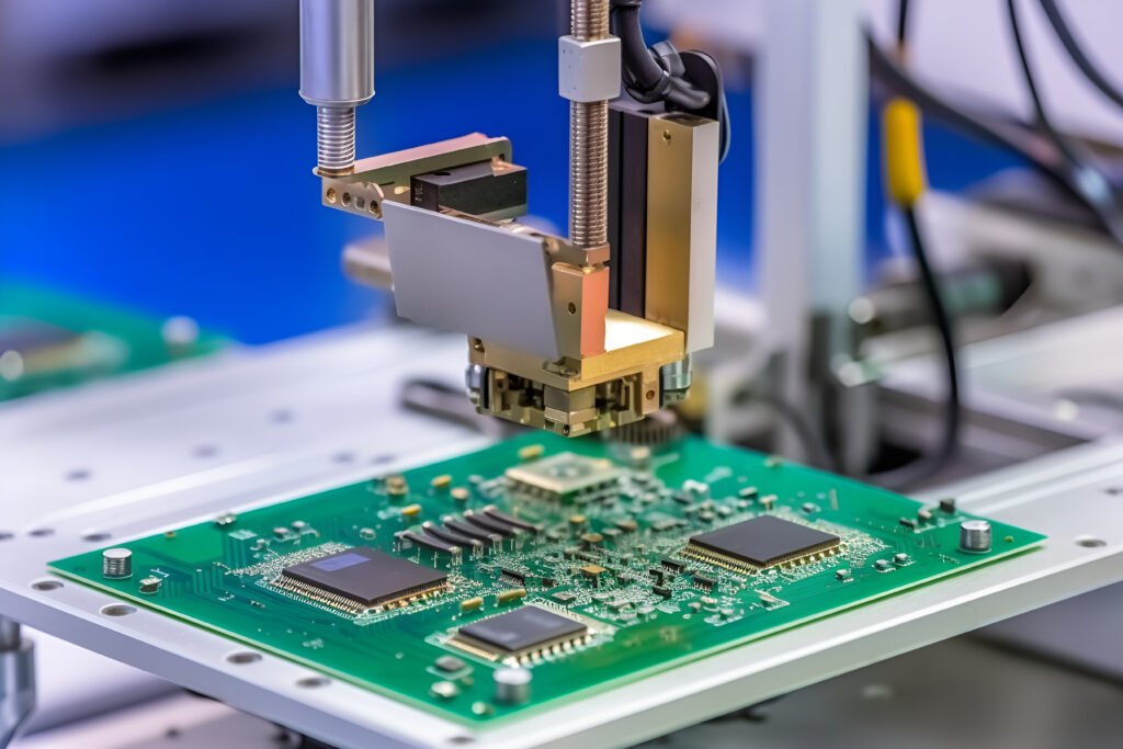
In the evolution of PCB surface treatment processes, ENIG (Electroless Nickel Immersion Gold) is gradually becoming the core choice for high-end electronics (e.g., 5G communications, aerospace, medical devices) due to its excellent reliability and high compatibility.The core lies in the synergy between the nickel layer as a mechanical barrier and the gold layer as a conductive medium.In this paper, we will analyse the unique value of ENIG from three aspects: technical principle, performance advantages and application scenarios.
I. Technical Analysis of the ENIG Process: Precision Design of Bimetallic Layers
The ENIG process is realised by a two-step chemical deposition:
1. Chemical Nickel Plating (Electroless Nickel)
- A uniform nickel-phosphorus alloy layer (typical thickness 3-5 μm) is formed on the copper surface using sodium hypophosphite reduction.
- The nickel layer not only provides mechanical support, but its phosphorus content (8-12%) significantly retards the diffusion of copper into the gold layer and prevents interfacial oxidation.
2. Immersion Gold
An ultra-thin gold layer of approximately 0.05-0.1μm is deposited on the nickel surface through a substitution reaction, where gold atoms directly replace nickel atoms on the nickel surface to form a dense cover.
Key parameter control:
The thickness of the gold layer directly affects the solder life and contact resistance (IPC standard recommends ≥0.05μm).
Synergistic mechanism:
- The nickel layer acts as a “sacrificial barrier” to isolate the copper from the external environment;
- The gold layer acts as a “conductive interface” to ensure solderability and signal integrity.
II. Core performance advantages of ENIG
1.Superreliability
- Corrosion resistance: The gold layer isolates oxygen and moisture, and the nickel-phosphorus alloy is resistant to acids and alkalis, which is suitable for offshore equipment and other harsh environments.
- Anti-migration: Nickel layer prevents the diffusion of copper ions, avoiding the risk of copper whiskers (Whisker) under the gold layer.
2.Excellent solderability and contactperformance
- Gold surface provides low contact resistance (<0.1Ω) to meet high frequency signal requirements (e.g. HDMI, RF circuits).
- Soldering life is up to 5 times or more (conventional hot air levelling is only 1-2 times).
3. Compatible with advancedprocesses
- Suitable for micro-pitch (<0.25mm) and BGA packages, avoiding the problem of pad cratering (compared to OSP process ).
- Supports multiple reflow (up to 260°C/10 seconds) to meet SMT high precision requirements.
III. Irreplaceability in high-end application scenarios
- 5G and millimetre-wave devices: ultra-low dielectric loss gold surface guarantees signal transmission stability.
- Aerospace and automotive electronics: nickel layer for high temperature resistance (up to 200°C continuous use) and vibration resistance.
- Medical implantable devices: biocompatible gold layers meet FDA approval requirements.
IV. Challenges and future trends
Although ENIG has higher cost (3-5 times more expensive than HASL) and the risk of Black Pad (caused by uneven phosphorus content), it has been significantly improved by process optimisation (e.g. low phosphorus nickel plating) and inspection technology (XRF thickness measurement).In the future, ENIG+OSP composite process may become a new direction to balance cost and performance.
Conclusion
ENIG’s nickel-gold bimetallic structure achieves a perfect balance between mechanical protection and electrical performance, and its technological maturity and reliability have enabled it to continue to lead in the high-end PCB field.With the development of electronic products towards high density and high frequency, the synergistic value of ENIG will be further highlighted.

 English
 中文
中文


